Bars
Bars
 Beads & Spheres
 Bolts & Nuts
 Crucibles
 Discs
Discs
 Fibers & Fabrics
 Films
Films
 Flake
Flake
 Foams
Foams
 Foil
Foil
 Granules
 Honeycombs
 Ink
Ink
 Laminate
 Lumps
Lumps
 Meshes
 Metallised Film
 Plate
Plate
 Powders
 Rod
Rod
 Single Crystals
 Sputtering Target
 Tubes
Tubes
 Washer
 Wires
Wires
 Converters & Calculators
 Write for Us

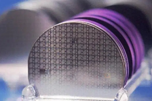
Graphene Transistors Made From DNA

In the world of electronics, smaller, cheaper and faster computer chips means better. Silicon has been popularized for a long time as a material used in making chips. As scientists continuously improve building smaller and higher speed chips, there comes a certain point that heat and other interfering factors interrupt some functions of silicon chips.
The primary running unit on a chip is the transistor. Transistors function as tiny gates for electric signals capable of amplification. At present, a promising technology may address the means for building smaller yet faster transistors with less power consumption. Stanford chemical engineering professor Zhenan Bao with her co-authors, former post-doctoral fellows Fung Ling Yap and Anatoliy Sokolov revealed the procedure of using DNA as a model to assemble the new generation of electronic chips based on this known wonder material-graphene, instead of silicon.
Bao and her colleagues believe that graphene’s physical and electrical properties could provide a very fast chip requiring only very little amount of power. Due to such thinness of graphene- one atom thick- and 20-50 atoms width, they came up with the idea of using DNA, which chemically contains carbon atoms, to provide a template for the graphene synthesis. DNA’s physical characteristics and organizational system let scientist assemble the graphene template proficiently.
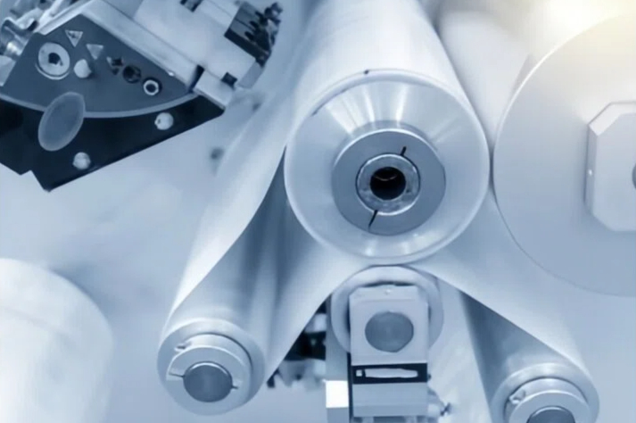
The Stanford team initiated the process by dipping a platter of silicon into a DNA rich solution then stretching out DNA strands by combing these homogenously straight. Afterwards, DNA on the platter was treated with a copper salt solution where copper ions were ingested into the DNA. The copper-doped DNA was then heated and bathed in hydrocarbon methane gas. The heat triggered in this procedure releases some carbon atoms which are formed into pure-carbon honeycomb of graphene.
According to Bao, the process is not yet perfect as not all of carbon atoms formed into honeycomb structures- some clustered into irregular patterns. Nevertheless, this low-cost technique, has great potential and could possibly replace silicon.
 Chin Trento