Bars
Bars
 Beads & Spheres
 Bolts & Nuts
 Crucibles
 Discs
Discs
 Fibers & Fabrics
 Films
Films
 Flake
Flake
 Foams
Foams
 Foil
Foil
 Granules
 Honeycombs
 Ink
Ink
 Laminate
 Lumps
Lumps
 Meshes
 Metallised Film
 Plate
Plate
 Powders
 Rod
Rod
 Single Crystals
 Sputtering Target
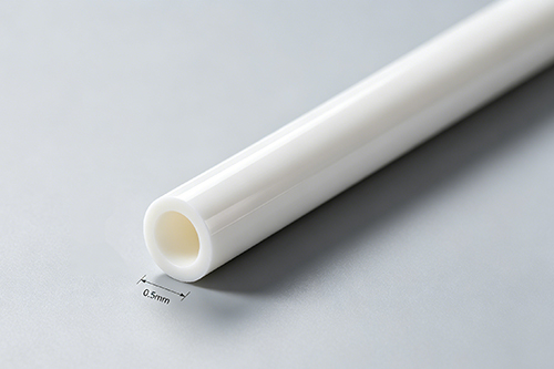
 Tubes
Tubes
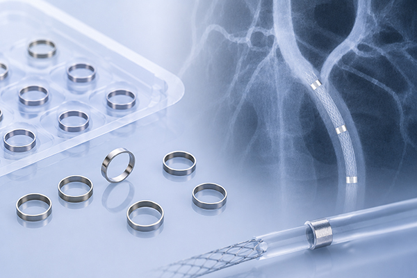
 Washer
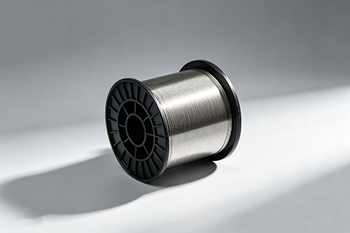
 Wires
Wires
 Converters & Calculators
 Write for Us

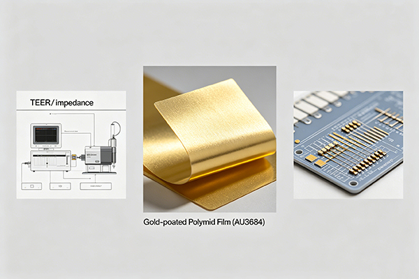
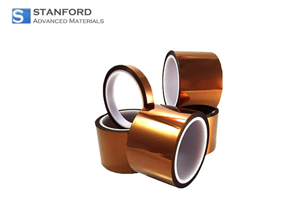
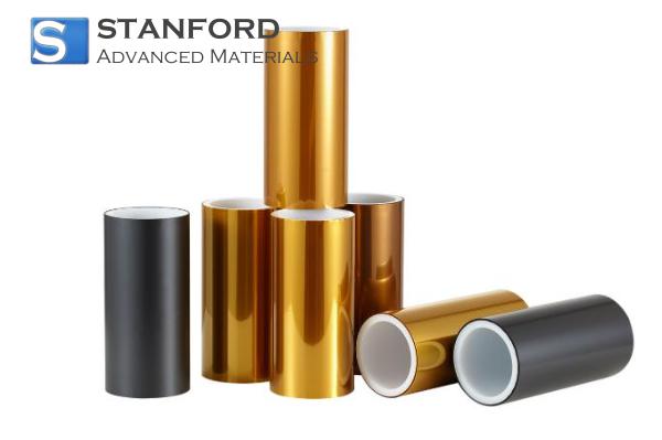
Gold-Plated Polyimide Film for TEER Impedance Measurements in Microfluidic R&D

Customer Background
A medical device R&D team was working on a microfluidic platform for transepithelial electrical resistance, or TEER, and general impedance measurements. Their device concept used thin electrode structures integrated into a compact fluidic chip, so the electrode material had to be conductive, chemically stable, and compatible with repeated contact with cell media.
They had already validated the basic chip geometry. What slowed them down was the electrode substrate. Conventional metal foils were too stiff, and some polymer-backed materials showed coating variation that made the electrical response drift from sample to sample. During initial testing, we noticed their biggest concern was not raw conductivity alone. It was consistency. Small changes in coating thickness or substrate flatness were enough to alter measured impedance and make the data harder to compare across test runs.
They needed small evaluation samples, not production volume, and they needed them quickly.
Challenge
The project had a few practical constraints that are common in early-stage medical R&D, but hard to solve cleanly.
The team needed a gold-plated polyimide film with a uniform Au layer, stable adhesion, and enough flexibility to fit into a microfluidic stack without cracking or curling. Their target sample format was small, but the electrode area still had to remain usable for TEER readings. They were working with a PI substrate around 50 µm thick, with a gold coating controlled tightly enough to keep sheet resistance from wandering between samples. They also asked for sample pieces cut to a specific width tolerance so they could drop them into their fixture without rework.
A second issue was compatibility. The film had to tolerate exposure to aqueous media and routine lab handling without edge flaking or visible delamination. One supplier had offered a plated film that looked acceptable on paper but arrived with slight edge damage from packing and handling. That was enough to invalidate a few bench trials.
Lead time was also tight. Their development schedule was tied to a round of electrode testing, and they could not wait through a long custom run just to evaluate the material.
Why They Chose SAM
The team contacted Stanford Advanced Materials (SAM) because they wanted a supplier that already understood thin film materials and controlled evaluation lots. We have spent decades supplying advanced materials to engineering groups, so the conversation started with practical details rather than generic promises.
Our team could provide small sample quantities, which mattered. They did not want to commit to a full production order before confirming electrode behavior in their microfluidic geometry. We also confirmed that the gold plating could be prepared with consistent thickness across the sheet and that the polyimide base would be kept flat enough for lab assembly. That sounded simple, but in thin-film work, the handling is often where problems start.
Another reason they chose SAM was responsiveness. They needed a material partner who could answer questions on coating stack-up, packaging, and sample sizing without turning the process into a long procurement loop. SAM was able to do that.
Solution Provided
We supplied gold-plated polyimide film samples prepared for early-stage TEER and impedance testing. The PI substrate was selected for thermal stability and flexibility, while the gold layer provided the electrode surface needed for low-noise measurements.
A few technical details mattered here. The film was prepared with a controlled polyimide thickness and a consistent gold coating thickness across the usable area. The sample pieces were cut to the requested evaluation size, and we kept the edge condition clean to avoid handling damage during chip assembly. We also packaged the film with interleaving protection so the coated surface would not rub during shipment.
Our team paid attention to the practical side of the request as well. The customer's fixture was sensitive to slight dimensional variation, so we kept the sample geometry within a narrow tolerance band. During preparation, we noticed that overly tight stacking in packaging could leave a minor curl at the corners of thin PI films. That suggested a simple adjustment in how the samples were supported in transit. After that change, the pieces arrived flatter and were easier to place into the test assembly.
For the coating itself, the main goal was not a decorative finish. It was electrical repeatability. The gold surface needed to support impedance measurements without introducing unpredictable contact resistance or local defects. We verified that the film was suitable for downstream prototyping and shared the relevant material data before shipment.
Results & Impact
Once the samples were integrated into the microfluidic test setup, the engineering team was able to run TEER and impedance measurements with less sample-to-sample variation than they had seen with earlier materials. The electrode response was more stable, and the lab spent less time compensating for material inconsistency during early validation.
A few outcomes stood out. The film handled routine wet-lab assembly without visible coating damage. The consistent Au layer gave the team a more repeatable electrical baseline across multiple evaluation samples. And because the substrate remained flexible but dimensionally usable, the electrodes fit their chip stack without forcing redesign of the carrier geometry.
The practical value was just as important as the test results. Small evaluation lots let them compare designs without tying up budget in a larger order. That reduced risk in the development phase. It also let the engineers move faster between iterations, which is often where medical device programs gain or lose time.
Stanford Advanced Materials (SAM) supported the work with a material that was simple on the surface but controlled where it mattered. That is usually the difference between a sample that looks right and one that actually behaves right in the lab.
Key Takeaways
Early-stage TEER and impedance projects depend on more than conductivity. Substrate handling, coating uniformity, packaging, and sample geometry all affect whether the material is useful in a real test fixture.
In this case, gold-plated polyimide film gave the team a practical electrode platform for microfluidic evaluation, and the small sample format reduced waste during R&D. SAM's ability to supply controlled thin-film materials in sample quantities helped the customer keep testing on schedule and avoid rework caused by unstable material behavior.
For labs developing electrode-based medical devices, that kind of consistency is often the part that keeps the program moving.
 Dr. Samuel R. Matthews