Bars
Bars
 Beads & Spheres
 Bolts & Nuts
 Crucibles
 Discs
Discs
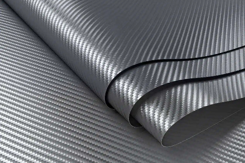
 Fibers & Fabrics
 Films
Films
 Flake
Flake
 Foams
Foams
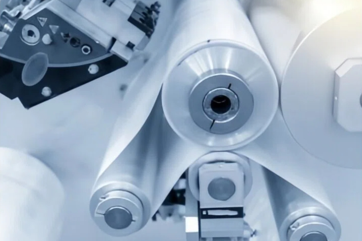
 Foil
Foil
 Granules
 Honeycombs
 Ink
Ink
 Laminate
 Lumps
Lumps
 Meshes
 Metallised Film
 Plate
Plate
 Powders
 Rod
Rod
 Single Crystals
 Sputtering Target
 Tubes
Tubes
 Washer
 Wires
Wires
 Converters & Calculators
 Write for Us

Nanotechnology Enables Creation of Printable Smart Phones

A group of Australian engineers has structured a type of laser known as spaser according to a news article published in ACS Nano journal. The spaser will enable manufacturers make very small and flexible smartphones. Spacers can be defined as nanoscale lasers the produce a light beam when free electrons vibrate. The beam produced by a traditional laser on the other hand consumes a lot of space. The new spaser discussed in the report will be made from carbon unlike earlier ones that were made from Plasmon amplification obtained from stimulating radiation emissions.
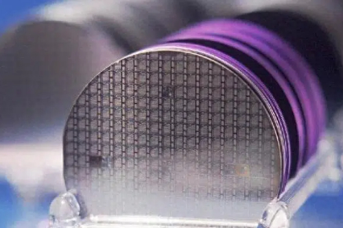
The kinds of spacers that we have seen in the recent days are manufactured from silver and gold nanoparticles or semiconductor quantum dots. The spasers assembled by the Australian engineers are made up of a carbon nanotube gain building block and a graphene resonator. According to the lead engineer, the spasers are expected to be stronger and more flexible, eco-friendly and able to withstand high temperatures because they are made from carbon. These properties might pave way for incredibly thin mobile that can be printed on a cloth in the future. Gadgets based on the spaser technology are expected to replace the current device components that are transistor-based such as displays, memory, and microprocessors. This will address the existing bandwidth and miniaturizing limitations.
According to the article, the spaser will be made from carbon nanotubes and graphene that are more than 100 times harder than steel and have excellent thermal and electrical conductivity. They can also withstand extremely high temperatures. In addition, the two carbon materials used for the spaser can interconnect and transfer energy to another through light. Since these visual relationships are very rapid and energy-efficient, it makes them appropriate for computer processors and other applications. Chanaka, the leading engineer also says that graphene and carbon have been tested with nanoscale antennas, waveguides and electric conductors to ensure that they possess the required optical, mechanical and electrical properties.
Many institutions have shown interest in spaser technology, are directing their investments to research, and develop the new technology. As a result, the Georgia State University is set to open a ‘Center for Nano Coptics.’ This center is expected to be a great milestone in the research for nanoplasmic metal funnel and spaser technology which is expected to form the future of small and printable smartphones. They are also viewing other options such as cancer treatment.
 Chin Trento