Bars
Bars
 Beads & Spheres
 Bolts & Nuts
 Crucibles
 Discs
Discs
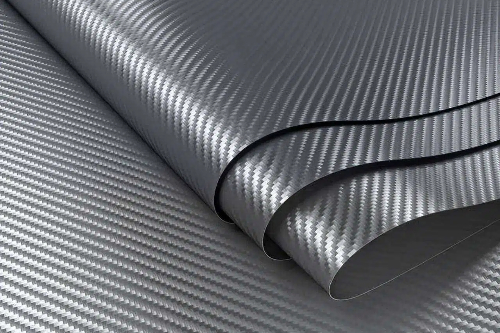
 Fibers & Fabrics
 Films
Films
 Flake
Flake
 Foams
Foams
 Foil
Foil
 Granules
 Honeycombs
 Ink
Ink
 Laminate
 Lumps
Lumps
 Meshes
 Metallised Film
 Plate
Plate
 Powders
 Rod
Rod
 Single Crystals
 Sputtering Target
 Tubes
Tubes
 Washer
 Wires
Wires
 Converters & Calculators
 Write for Us

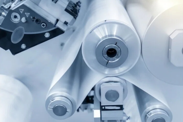
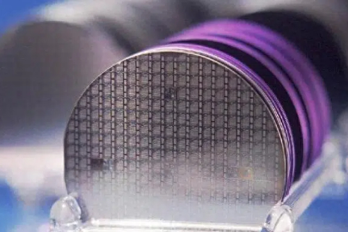
What is Sputtering?
Last updated on {{lastDate}}

Sputtering is a process that uses gaseous plasma to dislodge atoms from the surface of a solid target material. The atoms are deposited to form an extremely thin coating on the surface of the substrates. It is a technique often used to deposit thin films of semiconductors, CDs, disk drives, and optical devices. Sputtered films exhibit excellent uniformity, density, purity and adhesion. It is possible to produce alloys of precise composition with conventional sputtering, or oxides, nitrites and other compounds by reactive sputtering.
Process of sputtering:
- Ions of inert gas are accelerating into target
- Target is eroded by the ions via energy transfer and is ejected in the form of neutral particles
- Neutral particles from the target traverse and are deposited as a thin film onto the surface of the substrates

 Chin Trento