Bars
Bars
 Beads & Spheres
 Bolts & Nuts
 Crucibles
 Discs
Discs
 Fibers & Fabrics
 Films
Films
 Flake
Flake
 Foams
Foams
 Foil
Foil
 Granules
 Honeycombs
 Ink
Ink
 Laminate
 Lumps
Lumps
 Meshes
 Metallised Film
 Plate
Plate
 Powders
 Rod
Rod
 Single Crystals
 Sputtering Target
 Tubes
Tubes
 Washer
 Wires
Wires
 Converters & Calculators
 Write for Us

DC Sputtering: For Conductive Materials

This article is part of the PVD Basics series. Start here or view all articles.
The Short Answer
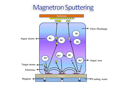
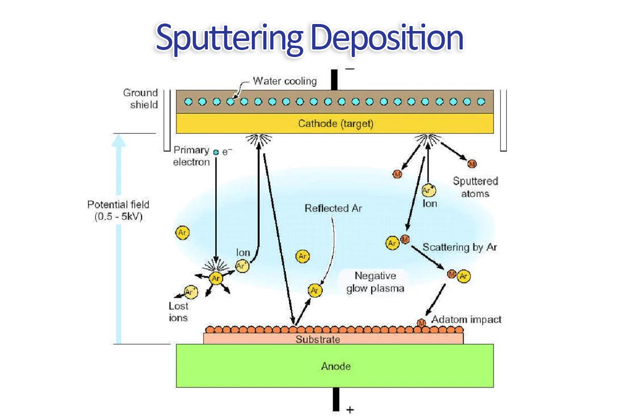
DC sputtering (Direct Current sputtering) is the simplest form of sputtering. A constant negative voltage is applied to the target. The target acts as a cathode. The chamber walls or substrate holder act as the anode. The DC voltage creates a plasma, and positive argon ions bombard the target to knock atoms loose.
It only works on conductive materials—metals and some semiconductors. For insulators, DC sputtering fails because charge builds up on the target surface.
If you need to deposit aluminum, copper, titanium, platinum, gold, or any other conductive metal, DC sputtering is the simplest, cheapest, and most reliable method.
How DC Sputtering Works
The setup is straightforward.

Schematic diagram of a DC sputtering system. Ardila Tellez, Luis & Orozco-Hernández, G. & Estupiñan, Fredy & Moreno-Téllez, Carlos-Mauricio & Olaya-Florez, Jhon-Jairo. (2023). Review of Nitride-Based Multifunctional PVD-Deposited Coatings. Revista Científica. 46. 162-176. 10.14483/23448350.20093.
A DC power supply connects to two electrodes inside a vacuum chamber. The target—the material you want to deposit—is attached to the cathode (negative terminal). The substrate sits on or near the anode (positive terminal), which is often the chamber body itself.
Argon gas is introduced at low pressure, typically 5 to 30 mTorr.
When you apply DC voltage—usually 300 to 1,000 volts—the electric field ionizes the argon gas. Electrons are pulled toward the anode (positive). Argon ions are pulled toward the cathode (negative).
The argon ions strike the target surface, knocking atoms loose. Those atoms travel through the chamber and land on the substrate, forming a thin film.
That is all. No magnets (though most modern DC sputtering systems add them). No RF matching. No complex waveforms. Just a steady DC voltage and a conductive target.
Why DC Sputtering Does Not Work for Insulators
This is the single most important limitation to understand.
An insulator does not conduct electricity. When argon ions strike an insulating target, their positive charge cannot be neutralized. Electrons from the power supply cannot flow through the target to reach the surface.
The result: positive charge builds up on the target surface. Eventually, the accumulated charge repels incoming argon ions. Sputtering stops. Then, when the voltage builds high enough, the charge discharges in an arc—a sudden, violent event that can send particles flying onto your substrate.
This is not a minor issue. DC sputtering simply does not work for insulators. You need RF sputtering for those materials.
Conductive Materials You Can DC Sputter
Almost any metal works.
Common DC sputtering targets:
|
Material |
Typical Application |
|
Semiconductor interconnects |
|
|
Chip wiring, PCB seed layers |
|
|
Adhesion layers, biomedical coatings |
|
|
Electrodes, Schottky contacts |
|
|
Electrical contacts, corrosion protection |
|
|
Diffusion barriers |
|
|
Magnetic films, underlayers |
|
|
Hard coatings, decorative finishes |
|
|
Reflective coatings, antimicrobial surfaces |
|
|
Transparent conductive films (semi-conductive, works with DC) |
If it conducts electricity, you can DC sputter it.
Advantages of DC Sputtering
Simple and inexpensive. DC power supplies cost much less than RF supplies. No impedance matching network is required. The setup is straightforward.
High deposition rates. DC sputtering is fast. For metals like aluminum or copper, deposition rates of 10 to 100 nm per minute are common.
Stable and reliable. Once the plasma ignites, DC sputtering runs steadily. No frequency tuning. No waveform adjustments. Set the power and go.
Scalable. DC sputtering works for 1-inch research targets and 10-foot architectural glass targets. Large-area DC sputtering is a mature, well-understood technology.
Low substrate heating. Like all sputtering, most energy stays in the plasma near the target. Temperature-sensitive substrates can be coated.
Limitations of DC Sputtering
Conductive materials only. This is the hard limit. No insulators. No ceramics. No oxides or nitrides (unless they are conductive).
Arcing can occur. Even with conductive targets, arcing happens. Surface contamination, rough target surfaces, or flakes from shields can trigger arcs. Modern DC power supplies have arc suppression, but arcing remains a source of particles.
Poor target utilization in planar systems. Like all planar magnetron sputtering, DC sputtering suffers from the racetrack erosion pattern. Only 25-35% of the target is used. The rest is wasted.
Not ideal for reactive sputtering. If you want to deposit an oxide or nitride by introducing oxygen or nitrogen gas, DC sputtering can suffer from "target poisoning"—the target surface reacts with the gas and becomes insulating, which then causes arcing. Pulsed DC or RF is often better for reactive processes.
DC Sputtering vs Other Power Types
|
Power Type |
Works For |
Speed |
Complexity |
Cost |
|
DC |
Conductors (metals) |
High |
Low |
Low |
|
Pulsed DC |
Conductors, some reactive processes |
High |
Medium |
Medium |
|
RF |
Conductors and insulators |
Medium |
High |
High |
|
HiPIMS |
Conductors (dense, ionized films) |
Low to medium |
High |
High |
If you are only depositing metals, DC sputtering is the right choice. If you need to deposit insulators or run reactive processes, look at RF or pulsed DC.
Typical Process Parameters
For a standard DC sputtering process:
|
Parameter |
Typical Range |
|
Voltage |
300 - 1,000 V |
|
Current density |
5 - 50 mA/cm^2 |
|
Power density |
1 - 20 W/cm^2 |
|
Pressure |
5 - 30 mTorr (argon) |
|
Base pressure |
< 5 × 10^-6 Torr |
|
Substrate temperature |
Ambient to 500°C (depending on system) |
These vary widely by material and system. Always run process development on your specific equipment.
Common Applications

Semiconductor manufacturing. DC sputtering deposits aluminum, copper, titanium, and tantalum layers. It is the standard method for metal deposition in chip fabrication.
Thin-film solar cells. DC sputtering deposits molybdenum back contacts, transparent conductive oxides, and metal grid lines.
Architectural glass. Large DC sputtering systems coat glass panels with low-emissivity (low-E) layers—typically silver-based stacks for energy-efficient windows.
Decorative coatings. Gold-colored TiN, black CrN, and other decorative finishes can be deposited by DC sputtering using metal targets in reactive gas.
Research and development. DC sputtering is common in university and industrial labs because the equipment is affordable and simple to operate.
A Note on Pulsed DC
Pulsed DC is a variation worth knowing.
Instead of a constant DC voltage, pulsed DC rapidly switches the voltage on and off—typically at frequencies of 20 to 350 kHz. The pulses are still unidirectional (always negative on the target), but the off-time allows charge to dissipate from the target surface.
This helps with reactive sputtering. When you introduce oxygen or nitrogen, the target surface can form an insulating compound layer. Pulsed DC prevents charge buildup and reduces arcing.
For pure metal sputtering in inert gas, standard DC is fine. For reactive sputtering of oxides and nitrides, consider pulsed DC.
The Bottom Line
DC sputtering is the simplest, fastest, and most economical way to deposit conductive thin films. It works for almost any metal, runs reliably, and scales from lab to production.
The limitation is clear: conductive materials only. For insulators, you need RF sputtering.
If you are depositing metals, start with DC sputtering. It has been the industry standard for decades for good reason.
Brought to you by Stanford Advanced Materials, a supplier of sputtering targets and evaporation materials.
 Dr. Samuel R. Matthews