Bars
Bars
 Beads & Spheres
 Bolts & Nuts
 Crucibles
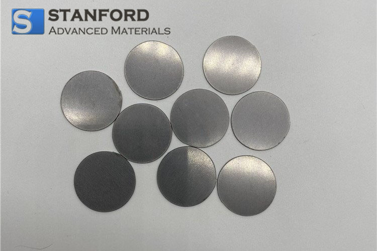
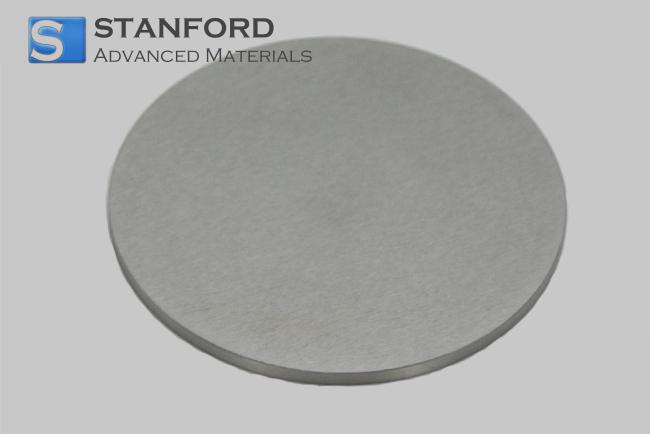
 Discs
Discs
 Fibers & Fabrics
 Films
Films
 Flake
Flake
 Foams
Foams
 Foil
Foil
 Granules
 Honeycombs
 Ink
Ink
 Laminate
 Lumps
Lumps
 Meshes
 Metallised Film
 Plate
Plate
 Powders
 Rod
Rod
 Single Crystals
 Sputtering Target
 Tubes
Tubes
 Washer
 Wires
Wires
 Converters & Calculators
 Write for Us

What is PVD? An Introduction to Physical Vapor Deposition

The Short Answer
Physical Vapor Deposition (PVD) is a family of techniques for creating thin films—layers of material just atoms or molecules thick. You take a solid material, turn it into vapor (usually by heating or by hitting it with ions), and let that vapor condense onto a surface to form a thin, solid layer.
It's how we put the metal lines on computer chips, the anti-reflective coating on eyeglasses, the gold-colored finish on watch cases, and the wear-resistant coating on drill bits.
One Sentence for Each Major PVD Method
PVD methods all follow the same basic idea—solid to vapor to film—but they get the vapor in different ways.
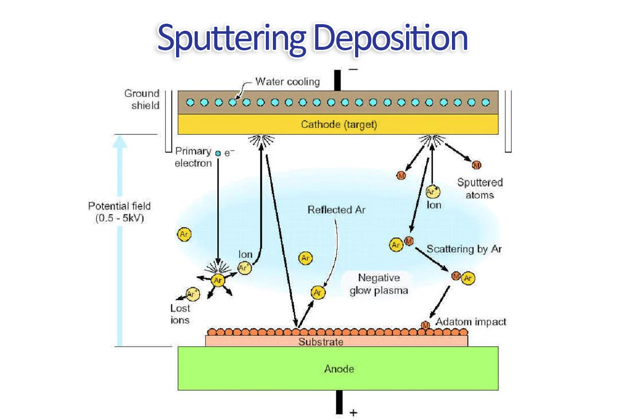
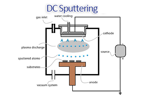
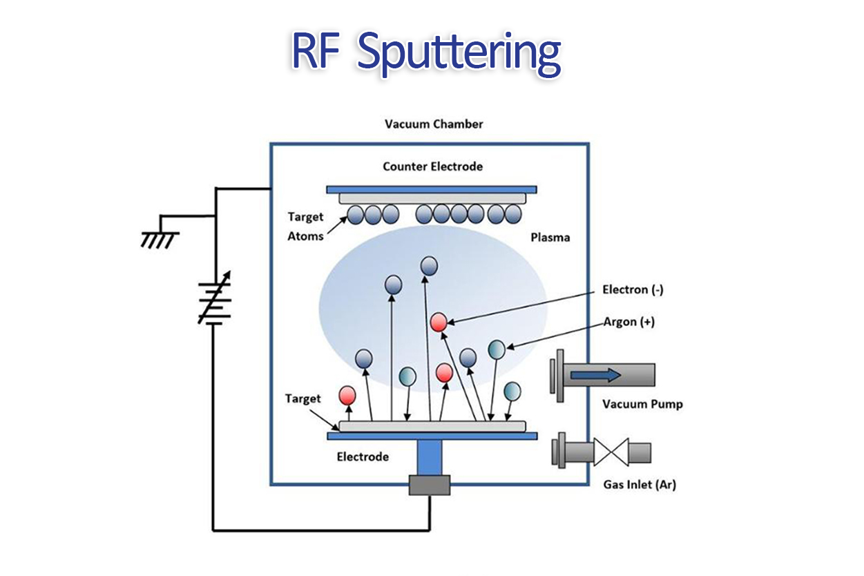
Sputtering uses high-energy ions to knock atoms off a solid target. The atoms fly through a vacuum chamber and land on the substrate. This is the most common PVD method in semiconductor manufacturing.
Evaporation heats a solid material until it turns to vapor. The vapor travels in a straight line to the substrate. This method is simpler and cleaner than sputtering but doesn't work well for high-melting-point materials.
Pulsed Laser Deposition (PLD) fires a high-power laser at a solid target. The laser creates a plasma plume of material that deposits onto the substrate. This method is less common in production but excellent for research on complex materials.

There are other variations—ion beam sputtering, reactive sputtering, HiPIMS—but they are refinements of these three core approaches.
What Makes PVD Different
PVD is not the only way to make thin films. You might also consider electroplating or Chemical Vapor Deposition (CVD). Here's how PVD compares.
PVD vs electroplating. Electroplating uses liquid chemicals and electricity. It is cheap and fast for thick films but produces chemical waste and works only on conductive substrates. PVD is dry, cleaner, and works on almost any material—but it costs more and requires vacuum equipment.
PVD vs CVD. CVD uses chemical reactions to grow films from gases. It can coat complex shapes evenly. But it runs at high temperatures and uses reactive, sometimes hazardous, gases. PVD runs cooler and uses no toxic precursors, but it struggles to coat the sides of deep holes or complex 3D shapes.
If you need a simple rule: PVD for line-of-sight coatings on flat or gently contoured surfaces. CVD when you need to coat deep trenches or complex shapes.
Where You Find PVD Every Day
You interact with PVD-coated products constantly, even if you don't know it.
Electronics. The metal layers in your phone's processor are deposited by sputtering. So are the reflective layers in DVDs and Blu-ray discs, and the electrodes in MEMS sensors.
Optics. Anti-reflective coatings on glasses, mirrors in telescopes, and filters in projectors are all made by evaporation or sputtering.
Tool coatings. Drill bits, end mills, and cutting inserts use PVD coatings (like titanium nitride) to last longer and run faster.
Decorative coatings. The gold color on watch cases, the black finish on bathroom fixtures, and the chrome look on plastic car trim are often PVD.
Medical devices. Implants, surgical tools, and stents use PVD coatings for wear resistance and biocompatibility.

The Basic PVD Workflow
Almost every PVD process follows the same five steps:
-
Clean the substrate. Any contamination on the surface will ruin adhesion. This step matters more than almost anything else.
-
Load the chamber. Place the substrate and the source material (target for sputtering, crucible for evaporation) inside the vacuum chamber.
-
Pump down to vacuum. Air molecules would block or react with the vapor. Typical pressures range from 10⁻³ to 10⁻⁷ Torr depending on the method.
-
Generate vapor. Apply energy—plasma ions, heat, or laser—to turn the source material into vapor.
-
Deposit the film. The vapor travels through the chamber and condenses on the substrate, forming a thin film.
Some processes add steps: heating the substrate, applying a bias voltage, or introducing a reactive gas (like oxygen or nitrogen) to form compounds.
What This Series Will Cover
This series covers PVD methods in practical detail. Each article focuses on what engineers actually need to know: how it works, where it excels, where it fails, and how to choose.
Sputtering methods: Magnetron, DC, RF, Reactive, Ion Beam, HiPIMS
Evaporation methods: Electron Beam, Thermal
Comparisons: PVD vs CVD, E-beam vs Thermal, Planar vs Rotary, DC vs RF
Practical topics: Coating colors, thin film stress, target bonding
If you already know which method you need, jump to that article. If you're just starting, the next article in this series covers magnetron sputtering—the most common PVD method in production today.
The Bottom Line
PVD is a dry, vacuum-based method for making thin films. It works on almost any substrate material, produces pure and dense films, and is the standard for electronics, optics, and tool coatings.
The trade-offs are equipment cost and line-of-sight limitations. But for the right applications, nothing else comes close.
Brought to you by Stanford Advanced Materials, a supplier of sputtering targets and evaporation materials.
 Dr. Samuel R. Matthews