Bars
Bars
 Beads & Spheres
 Bolts & Nuts
 Crucibles
 Discs
Discs
 Fibers & Fabrics
 Films
Films
 Flake
Flake
 Foams
Foams
 Foil
Foil
 Granules
 Honeycombs
 Ink
Ink
 Laminate
 Lumps
Lumps
 Meshes
 Metallised Film
 Plate
Plate
 Powders
 Rod
Rod
 Single Crystals
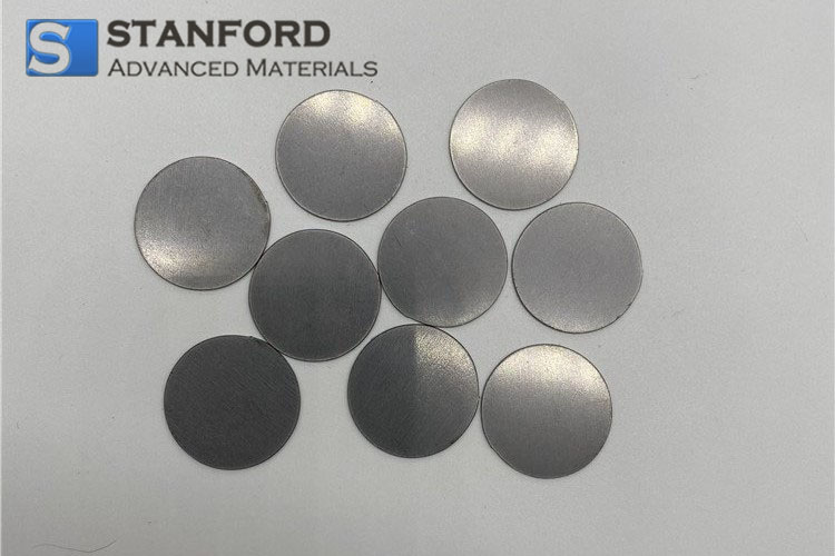
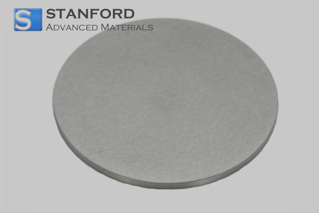
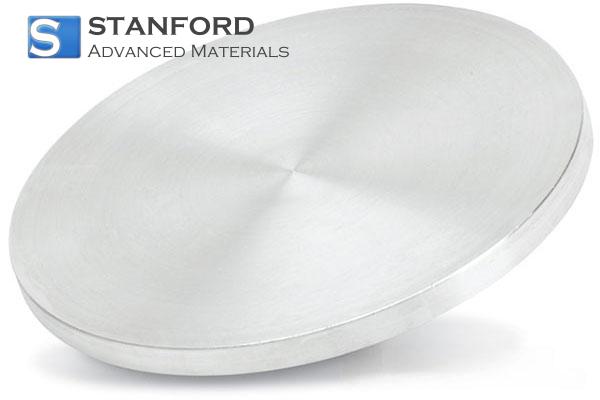
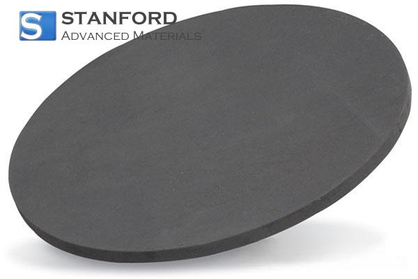
 Sputtering Target
 Tubes
Tubes
 Washer
 Wires
Wires
 Converters & Calculators
 Write for Us

Sputtering Deposition: How It Works and Where It's Used

This article is part of the PVD Basics series. Start here or view all articles.
The Short Answer
Sputtering deposition is a PVD method that uses energetic ions to knock atoms off a solid target. Those atoms then travel through a vacuum chamber and condense onto a substrate to form a thin film.
Unlike evaporation, which heats material until it turns to vapor, sputtering uses a physical momentum transfer process—like a microscopic game of billiard balls. This difference gives sputtering unique advantages: better adhesion, precise composition control for alloys, and the ability to deposit high-melting-point materials.
If you need dense, well-adhering films from almost any solid material—metal, alloy, ceramic, or semiconductor—sputtering is likely the right choice.

Scheme of the sputtering deposition process. Martins, R.M.S.. (2008). In-situ X-Ray diffraction studies during growth of Ni-Ti Shape Memory Alloy films and their complementary ex-situ characterization.
How Sputtering Works
The word "sputtering" describes the physical process. Here is what happens step by step.
Step 1: Create a plasma. A vacuum chamber is filled with a small amount of inert gas—almost always argon. A high voltage applied between a target (cathode) and the chamber walls or substrate holder (anode) ionizes the argon gas, creating a plasma.
Step 2: Accelerate ions. The positively charged argon ions are attracted to the negatively charged target. The voltage difference accelerates them.
Step 3: Knock atoms loose. When an argon ion strikes the target surface, it transfers its momentum. If the transfer is large enough, a target atom is ejected. One incoming ion can knock out multiple target atoms through a collision cascade.
Step 4: Transport through vacuum. The ejected target atoms travel through the vacuum chamber. At typical sputtering pressures (a few millitorr), they travel in nearly straight lines with few gas collisions.
Step 5: Condense on substrate. The atoms arrive at the substrate and condense to form a thin film. The energy of arriving atoms—much higher than in evaporation—helps them move on the surface and form dense, well-adhering films.
That is sputtering. No melting. No evaporation. Just atoms knocked loose by ion impact.
A Simple Way to Think About It
Imagine a billiard ball (an argon ion) slamming into a tightly packed rack of balls (the target surface). The impact sends several balls flying in different directions. Some of those balls land on the substrate.
Sputtering is momentum transfer, not thermal evaporation. This is why you can sputter materials that melt at 3,000°C—you never need to melt them.
Sputtering vs Evaporation: The Key Differences
These two PVD methods are often compared. Here is the practical difference.
|
Feature |
Sputtering |
Evaporation |
|
How atoms are ejected |
Ion impact (momentum) |
Heating (thermal) |
|
Energy of arriving atoms |
1-10 eV |
0.1-0.5 eV |
|
Film density |
High |
Moderate |
|
Adhesion |
Excellent |
Good but can be poor |
|
Composition control |
Exact (target matches film) |
May fractionate in alloys |
|
High-melting-point materials |
Easy |
Difficult or impossible |
|
Substrate heating |
Low to moderate |
Very low |
|
Step coverage |
Poor (line-of-sight) |
Poor (line-of-sight) |
|
Particle risk |
Moderate (arcing, target defects) |
Low |
The higher arrival energy in sputtering is the main advantage. Energetic atoms can rearrange on the substrate surface, fill voids, and form denser films with better adhesion.
The trade-off is complexity. Sputtering requires plasma generation and target management. Evaporation only needs a hot crucible.
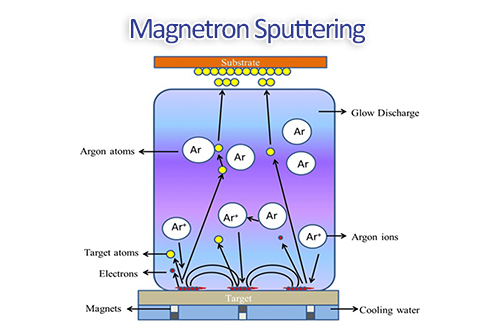
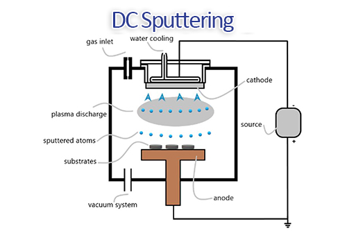
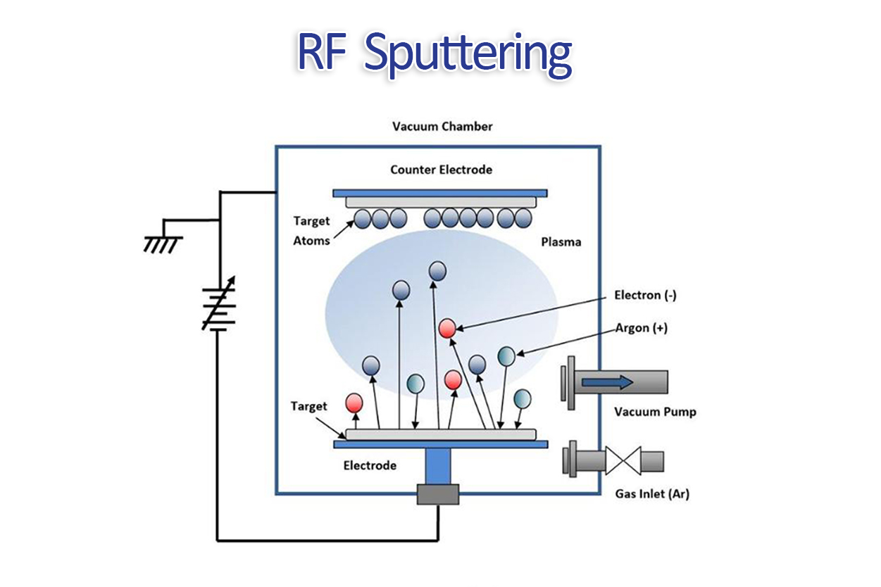
Types of Sputtering
Sputtering is not one technique. It is a family. The PVD Basics series covers each of these in separate articles.
|
Type |
Best For |
Key Limitation |
|
Conductive metals |
Does not work for insulators |
|
|
RF Sputtering |
Insulators and dielectrics |
Slower, more expensive |
|
Magnetron Sputtering |
High-rate production |
Poor target utilization |
|
Reactive Sputtering |
Oxides, nitrides, carbides |
Process control is tricky |
|
Ion Beam Sputtering |
Ultra-smooth, high-density films |
Very slow, expensive |
|
HiPIMS |
Dense, ionized films |
Complex, slower than DC |
If you are new to sputtering, start with magnetron sputtering (covered separately in this series). It is the most common production method. Then learn about DC and RF power supplies, since they determine what materials you can deposit.
What Affects Film Quality in Sputtering

Target purity. Lower purity means more impurities in your film. For semiconductor work, you need 99.95% or better. For decorative coatings, 99.9% is fine.
Target density. A dense target sputters cleanly. A porous target outgasses, arcs, and generates particles. Never buy a low-density target for critical work.
Base pressure. The pressure before you introduce argon. Higher base pressure means more residual water vapor and air in the chamber, which can oxidize your film or cause contamination. Aim for 10⁻⁶ Torr or better.
Sputtering pressure. Typical range is 2 to 20 mTorr. Lower pressure gives fewer gas collisions and more directional deposition. Higher pressure gives more scattering and can improve uniformity at the cost of rate.
Substrate bias. Applying a negative bias to the substrate attracts positive ions during deposition. This densifies the film and improves adhesion but can increase film stress.
Common Applications
Semiconductors. Metal layers (Al, Cu, Ti, Ta) and diffusion barriers (TiN, TaN) are sputtered. Sputtering dominates front-end and back-end metal deposition in chip manufacturing.
Hard drives. The magnetic recording layers and read/write head structures are sputtered. This is one of the largest-volume sputtering applications.
Optical coatings. Anti-reflective coatings, mirrors, and filters use sputtering when high density and durability are required.
Decorative coatings. Gold, black, and other colored finishes on watches, faucets, and automotive trim are often sputtered.
Solar cells. Transparent conductive oxides and metal contacts in thin-film solar cells use sputtering.
Tool coatings. TiN, AlTiN, and CrN coatings on cutting tools can be applied by sputtering, though arc evaporation is also common.

When to Choose Sputtering
Choose sputtering when:
-
You need dense, well-adhering films
-
Your material has a high melting point (tungsten, tantalum, platinum)
-
You need precise composition control in alloys
-
Your substrate cannot tolerate high temperatures
-
You need uniform films over large areas
Choose evaporation when:
-
You need the highest possible purity (no plasma or target impurities)
-
Your material has a low melting point (aluminum, gold, silver)
-
You want the simplest possible system
-
Substrate heating is a major concern
Limitations to Know
Line-of-sight deposition. Sputtering, like evaporation, is line-of-sight. It does not coat the sides of deep holes or complex 3D shapes well. For those applications, consider CVD.
Target utilization is poor in planar systems. The racetrack erosion pattern wastes 65-75% of the target. Rotary targets improve this but cost more.
Particle generation is a risk. Arcing, target defects, or flaking from shields can produce particles that cause defects. This is a constant battle in semiconductor sputtering.
Insulators require RF power. You cannot DC sputter an insulator. You need RF power, which is slower and requires impedance matching.
The Bottom Line
Sputtering deposition is a versatile, production-proven PVD method. It works for almost any solid material, produces dense films with excellent adhesion, and scales from research to high-volume manufacturing.
The main limitations are line-of-sight deposition and poor target utilization in planar systems. For many applications, these are acceptable trade-offs for the film quality and material flexibility sputtering provides.
If you are deciding between sputtering and evaporation, ask two questions: does your material have a high melting point, and do you need dense films? If yes to either, sputtering is likely your answer.
Brought to you by Stanford Advanced Materials, a supplier of sputtering targets and evaporation materials.
 Dr. Samuel R. Matthews