Bars
Bars
 Beads & Spheres
 Bolts & Nuts
 Crucibles
 Discs
Discs
 Fibers & Fabrics
 Films
Films
 Flake
Flake
 Foams
Foams
 Foil
Foil
 Granules
 Honeycombs
 Ink
Ink
 Laminate
 Lumps
Lumps
 Meshes
 Metallised Film
 Plate
Plate
 Powders
 Rod
Rod
 Single Crystals
 Sputtering Target
 Tubes
Tubes
 Washer
 Wires
Wires
 Converters & Calculators
 Write for Us

RF Sputtering: For Insulators and Dielectrics

This article is part of the PVD Basics series. Start here or view all articles.
The Short Answer
RF sputtering (Radio Frequency sputtering) is the method you use when your target is an electrical insulator. Unlike DC sputtering, which fails on insulators because of charge buildup, RF sputtering uses an alternating current at 13.56 MHz to neutralize the target surface with every cycle.
If you need to deposit oxides (SiO2, Al2O3, TiO2), nitrides (Si3N4, AlN), or any non-conductive ceramic, RF sputtering is the standard solution.
The trade-off is speed and complexity. RF sputtering is slower and requires more expensive equipment than DC sputtering. But for insulators, it is the only practical choice.
The Problem DC Has With Insulators
To understand RF sputtering, you first need to understand why DC fails.
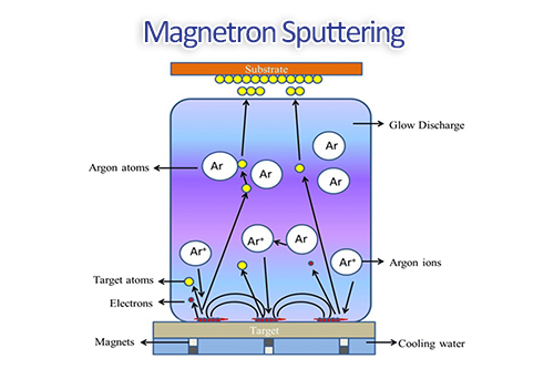
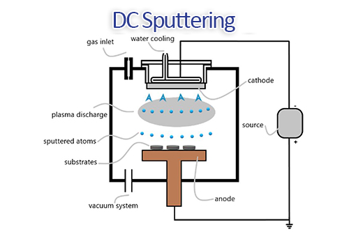
In DC sputtering, a constant negative voltage is applied to the target. Positive argon ions are attracted to the target. They strike it and knock atoms loose.
When the target is a metal, electrons from the power supply flow through the target to neutralize the arriving positive ions. No charge builds up.
When the target is an insulator, those electrons cannot flow. The target has no free electrons to move. The positive charge from the argon ions accumulates on the target surface. After a few microseconds, the surface becomes so positively charged that it repels any additional argon ions. Sputtering stops.
Then the voltage continues to rise until it finds a path to discharge—usually through an arc. The arc sends a shower of particles onto your substrate. Your film is ruined.
DC sputtering simply cannot deposit insulators.
How RF Sputtering Solves the Problem
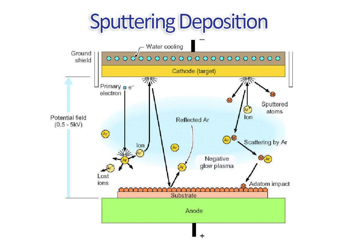
RF sputtering uses alternating current at a standard frequency of 13.56 MHz (the frequency allocated by regulations for industrial, scientific, and medical equipment).
. Device Fabrication and Characterization Techniques for Semiconductor Devices. DOI:10.13140/RG.2.2.14716.96642")
Schematic diagram of an RF sputtering system. Shashikant Sharma (2016). Device Fabrication and Characterization Techniques for Semiconductor Devices. DOI:10.13140/RG.2.2.14716.96642
Here is what happens during each cycle.
During the negative half-cycle. The target becomes negative. Argon ions are attracted to the target and strike it, knocking atoms loose. Sputtering happens. Positive charge begins to build up on the target surface.
During the positive half-cycle. The target becomes positive. Electrons from the plasma are attracted to the target. They neutralize the positive charge that built up during the negative half-cycle.
This happens 13.56 million times per second. The target surface never has time to accumulate significant charge. Sputtering continues steadily.
The positive half-cycle also bombards the target with electrons, which can cause secondary electron emission and heating. But the key point is this: charge never builds up, so arcing does not occur.
Why 13.56 MHz?
The frequency is not arbitrary. 13.56 MHz is an internationally regulated ISM band (Industrial, Scientific, Medical). Equipment operating at this frequency does not interfere with communications.
Lower frequencies would work electrically but might cause interference. Higher frequencies work but require more expensive components.
13.56 MHz is the standard. Every RF sputtering system you encounter will use this frequency. Power supplies, matching networks, and cables are all designed for it.
The Impedance Matching Challenge
RF sputtering has a complication that DC sputtering does not: impedance matching.
The plasma inside your chamber has a certain impedance—its resistance to the flow of RF power. This impedance changes as the plasma ignites, as the target erodes, and as gas pressure fluctuates.
Your RF power supply expects to see a specific impedance, typically 50 ohms. If the plasma impedance does not match, power reflects back into the generator instead of being delivered to the plasma. Reflected power can damage the generator.
The solution is an impedance matching network—a set of adjustable capacitors (and sometimes inductors) that sits between the power supply and the chamber. The matching network adjusts itself continuously to keep the impedance at 50 ohms.
This is why RF sputtering systems are more complex and expensive than DC systems. The matching network adds cost and is one more thing that can fail.
Advantages of RF Sputtering
- Works for any material. Conductor, semiconductor, insulator—RF sputtering handles everything. You can change from a metal target to an oxide target without changing power supplies.
- Dense, high-quality films. RF sputtering produces films that are typically denser and have fewer defects than DC-sputtered films. The energetic ion bombardment continues throughout deposition.
- Good adhesion. The plasma in RF sputtering is sustained at lower pressures than DC sputtering (1-15 mTorr vs 5-30 mTorr). Fewer gas collisions mean more energetic arriving atoms and better adhesion.
- Stable reactive sputtering. When depositing oxides or nitrides by introducing reactive gas, RF sputtering is more stable than DC. The alternating current helps prevent target poisoning.
Limitations of RF Sputtering
- Slower than DC. RF sputtering typically has lower deposition rates than DC sputtering for the same power. Some energy is lost in the matching network. The positive half-cycle does not contribute to sputtering.
- Higher cost. RF power supplies cost significantly more than DC supplies. The matching network adds more cost. A complete RF sputtering system can be two to three times the price of an equivalent DC system.
- More complex. Tuning the matching network, managing reflected power, and troubleshooting RF systems requires more expertise than DC sputtering.
- Heating. The electron bombardment during the positive half-cycle heats the target. For some materials, this can be an issue. For polymer or organic targets, RF sputtering may cause decomposition.
RF Sputtering vs DC Sputtering
|
Feature |
DC Sputtering |
RF Sputtering |
|
Works for insulators |
No |
Yes |
|
Deposition rate (metal) |
High (reference) |
30-50% of DC |
|
Equipment cost |
Low |
High (2-3x) |
|
Complexity |
Low |
High (matching network) |
|
Film density |
Good |
Very good |
|
Reactive sputtering stability |
Poor (arcing) |
Good |
|
Target heating |
Low |
Moderate to high |
The choice is simple: if you only deposit metals, use DC. If you need to deposit insulators or run stable reactive processes, use RF.
Materials Commonly Deposited by RF Sputtering
|
Material |
Type |
Application |
|
SiO2 (silica) |
Oxide |
Insulating layers in semiconductors, optical coatings |
|
Al2O3 (alumina) |
Oxide |
Wear-resistant coatings, electrical insulation |
|
TiO3 (titania) |
Oxide |
Optical coatings, photocatalysts |
|
Si3N4 (silicon nitride) |
Nitride |
Passivation layers, diffusion barriers |
|
AlN (aluminum nitride) |
Nitride |
Piezoelectric films, thermal conductors |
|
ITO (indium tin oxide) |
Transparent conductor |
Touch screens, solar cells (also works with DC) |
|
PZT (lead zirconate titanate) |
Ferroelectric |
MEMS sensors, actuators |
Many of these materials are impossible or very difficult to deposit by any other PVD method. RF sputtering is the standard for dielectric thin films.
Typical Process Parameters
For a typical RF sputtering process:
|
Parameter |
Typical Range |
|
Frequency |
13.56 MHz (fixed) |
|
Power |
50 - 1,000 W (depending on target size) |
|
Pressure |
1 - 15 mTorr (argon) |
|
Base pressure |
< 5 × 10^-6 Torr |
|
Reflected power |
< 5% of forward power |
|
Deposition rate (oxides) |
1 - 10 nm/minute |
Deposition rates for insulators are significantly lower than for metals. Plan accordingly.
Common Applications
Semiconductor manufacturing. RF sputtering deposits silicon dioxide (SiO2) and silicon nitride (Si3N4) layers in chip fabrication. These are critical insulating and passivation layers.
Optical coatings. Anti-reflective coatings, high-reflective mirrors, and interference filters often use RF-sputtered oxides (TiO2, SiO2, Ta2O5).
Piezoelectric devices. Aluminum nitride (AlN) and PZT films for MEMS sensors and actuators are typically RF-sputtered.
Thin-film capacitors. Dielectric layers in thin-film capacitors are often RF-sputtered oxides.
Research and prototyping. RF sputtering is common in labs because a single system can deposit metals, semiconductors, and insulators.
The Bottom Line
RF sputtering is the standard method for depositing insulating thin films. It works where DC sputtering fails—on oxides, nitrides, and all non-conductive materials.
The trade-offs are real: slower deposition, higher cost, and more complexity. But for insulators and dielectrics, RF sputtering is the only practical choice.
If your work involves any non-conductive thin films, you need RF sputtering capability. And once you have it, you can also use the same system for metal deposition—though at lower rates than DC.
Brought to you by Stanford Advanced Materials, a supplier of sputtering targets and evaporation materials.
 Dr. Samuel R. Matthews