Bars
Bars
 Beads & Spheres
 Bolts & Nuts
 Crucibles
 Discs
Discs
 Fibers & Fabrics
 Films
Films
 Flake
Flake
 Foams
Foams
 Foil
Foil
 Granules
 Honeycombs
 Ink
Ink
 Laminate
 Lumps
Lumps
 Meshes
 Metallised Film
 Plate
Plate
 Powders
 Rod
Rod
 Single Crystals
 Sputtering Target
 Tubes
Tubes
 Washer
 Wires
Wires
 Converters & Calculators
 Write for Us

Gallium Arsenide Wafer VS. Silicon Wafer

Introduction
With the development of electronic devices, people pay more and more attention to wafers, chips, semiconductors, and integrated circuits. Everyone is trying to figure out the essence of chips. Their mind is full of questions. What is a wafer? What is a chip? What about their relations? What materials do we use to make them? What are their cons and pros? This article is going to answer these questions by comparing gallium arsenide wafers and silicon wafers. Hope that you can have a clearer understanding of them.
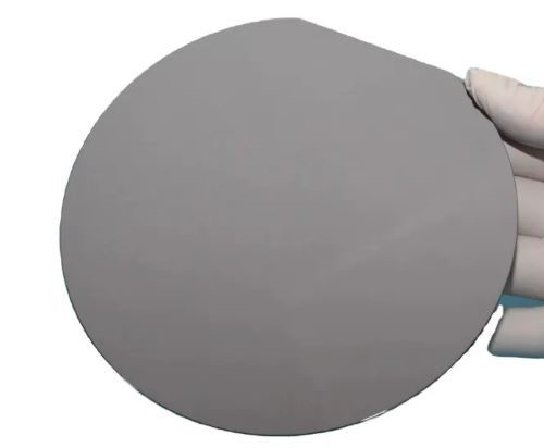
Figure 1 Gallium Arsenide Wafers
Wafers & Chips
- What is a wafer?
A wafer is a thin slice of semiconductor used to fabricate integrated circuits and other important electronic devices. The wafer is the base of integrated circuits. Both wafers and integrated circuits are regarded as the heart of the electronic industry.
- What is a chip?
A chip, an integrated circuit or an IC, is a group of electronic circuits embedded in one piece of semiconductor material. A range of mini-transistors and electronic components are put together on chips.
- What about their difference?
The wafer is the substrate for the chip. The chip is integrated into the wafer. They are set together and extensively employed in the electronics sector.
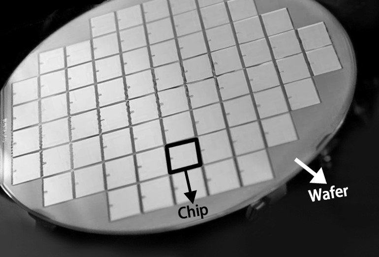
Figure 2. Chips on the Wafer
Gallium Arsenide Wafer VS. Silicon Wafer
--Silicon Wafers
- Pros:
Traditionally, silicon is the choice material for wafers because of the following benefits. The principal advantage of silicon wafers lies in their cost. Namely, it is much cheaper than other materials, and it takes up over 90% of the semiconductor market nowadays. Silicon wafers also have wide applications because of their ideal current and voltage handling capacity.
- Cons:
However, silicon could not meet customers’ demands when they require larger-size wafers. Silicon is a brittle material since all the atoms are aligned into a single crystal form. It is rarely used to make large-size wafers because they might crack. If we increase the thickness of the wafer to prevent breakage, the cost would increase accordingly, and silicon will lose its price advantage.
--Gallium Arsenide Wafers
- Pros:
Currently, gallium arsenide wafers arise as an alternative to silicon wafers. GaAs wafers have several technical advantages. They are listed below.
- First, electrons move much faster inside gallium arsenide wafers than they could inside silicon. So, this arsenide is widely used to make high-speed telecommunication devices.
- Second, gallium arsenide wafers have the unique ability to turn electricity into light. This notable optical property contributes to the extensive applications in laser diodes, optical windows, solar cells, and other optoelectronics.
- Gallium arsenide-based devices have much more benefits. GaAs has a lower saturation field and a broader operating temperature range compared with silicon. GaAs wafers could also reduce noises in electronic circuits.
- Cons:
Nevertheless, gallium arsenide wafers have the following drawbacks.
- Gallium arsenide is more costly than silicon since GaAs are much rarer and harder to get. But its higher efficiency justifies the higher cost. Gallium arsenide wafers are usually employed in novel equipment or projects which have higher requirements and higher budgets.
- GaAs does not form native oxides like silicon, while silicon could use its oxides as an insulator to protect itself.
- Much caution is needed for the handling and disposal of gallium arsenide components because arsenic is very toxic.
Conclusion
Above all, both wafers and chips are of great importance to the semiconductor industry and the electronic industry, and various materials have been used to manufacture wafers. Silicon wafers are cheaper options, while gallium arsenide wafers are famous for their electron mobility, impressive optical feature, and higher efficiency. Stanford Advanced Material (SAM) provides single-crystal gallium arsenide wafers made by LEC and VGF methods. You can check our homepage for more information.
 Chin Trento