Bars
Bars
 Beads & Spheres
 Bolts & Nuts
 Crucibles
 Discs
Discs
 Fibers & Fabrics
 Films
Films
 Flake
Flake
 Foams
Foams
 Foil
Foil
 Granules
 Honeycombs
 Ink
Ink
 Laminate
 Lumps
Lumps
 Meshes
 Metallised Film
 Plate
Plate
 Powders
 Rod
Rod
 Single Crystals
 Sputtering Target
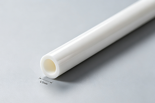
 Tubes
Tubes
 Washer
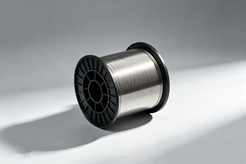
 Wires
Wires
 Converters & Calculators
 Write for Us

Optimized Copper Sputtering Targets for High-Volume Semiconductor Interconnect Manufacturing

Customer Background
A key engineer based in Brazil represents a semiconductor manufacturing company producing copper interconnects for advanced chips. With frequent batch orders and a clear vision for scaling up production of high-quality copper films, the customer required a solution that ensured consistency in sputtering processes while accommodating high-volume demands.
The customer typically uses copper sputtering targets for depositing conductive thin films critical for interconnect formation. In previous projects, standard targets occasionally resulted in variable film thickness and inconsistencies due to material variations. Their requirements demanded not only high-purity copper but also rigorous dimensional control and an optimized bonding configuration to handle thermal cycling during extended sputtering sessions.

Challenge
The main challenge lay in the demand for a sputtering target that could reliably support the high-volume deposition process without compromising uniformity and performance. Specific technical requirements included:
• Copper sputtering target purity of no less than 99.99% to minimize contaminants that could adversely affect film conductivity.
• Precise thickness and diameter specifications with a tolerance of less than ±0.05 mm to ensure uniformity across each target.
• An engineered bonding configuration between the copper target and its backing structure to improve thermal conductivity during rapid sputtering cycles.
")
Additionally, the customer faced a real-world constraint involving tight lead times—rapid production and delivery were essential as any delay in material supply would upset the assembly line and potentially affect yield reliability. Prior suppliers had struggled with achieving consistent quality and meeting these delivery schedules, which prompted the search for a partner capable of both design flexibility and technical precision.
Why They Chose SAM
Our team at Stanford Advanced Materials (SAM) engaged early with the client to understand the nuances of his production environment and the specific requirements of the semiconductor interconnect process. We reviewed the supplied specifications and highlighted several critical factors:
• We examined the interplay between target purity and deposition performance.
• We proposed modifications in the bonding process to address potential thermal instabilities during extended sputtering runs.
• We ensured that the mechanical tolerances could be consistently met even under high-volume production conditions.
This in-depth consultation, coupled with our 30+ years of experience in managing global supply chains and customizing material solutions for intricate processes, gave the customer confidence that SAM was the right partner to handle this challenging application.
Solution Provided
Our solution began with an in-depth evaluation of the copper material requirements. We selected copper with a verified purity of 99.99%, ensuring that the electrical properties needed for semiconductor interconnects would be maintained. Detailed spectrographic analysis and batch testing confirmed that the supplied copper met the stringent chemical composition criteria.
To tackle dimensional challenges, we employed precision machining methods, achieving a target thickness maintained within ±0.05 mm tolerances. This ensured that the sputtering deposition remained even across the entire surface area, contributing to a consistent film formation on the semiconductor wafers. We also worked on an optimized bonding strategy, where the copper target was bonded to a copper-backed support structure using a controlled thermo-mechanical process. This improved thermal dissipation during rapid cycling operations, significantly reducing the risk of microstructural variabilities over prolonged sputtering sessions.
In addressing the sensitivity of the semiconductor process to oxidation and surface irregularities, each target was packaged in a nitrogen-purged, vacuum-sealed container immediately after fabrication. This controlled packaging method prevented surface oxidation and minimized particulate contamination, a critical factor when the targets are integrated into high-precision sputtering systems.
Furthermore, we adjusted the target edge geometry to ensure compatibility with the clamping system in the customer's deposition equipment. This customization minimized any potential misalignment issues that could lead to uneven sputtering and subsequent defects in the copper film.
Results & Impact
Implementation of our copper sputtering target solution yielded measurable improvements. The high-purity copper targets demonstrated a reduced variability in film thickness across multiple runs during the scale-up phase. By maintaining a consistent deposition profile, the customer could achieve more reliable interconnect structures with improved conductivity and reduced electrical losses.
The bonding configuration further contributed to enhancing heat distribution across the target surface, resulting in lower thermal fluctuations during operation. This meant that even when pushing through high-volume orders, the targets maintained their performance, meeting the rigorous demands of semiconductor manufacturing.
Delivery lead times were upheld as scheduled, with our global supply chain network ensuring that production could scale up without any interruptions. The combination of precise machining, robust bonding methods, and optimal packaging provided a solid foundation for a repeatable and reliable sputtering process.
Key Takeaways
• Achieving high purity in sputtering targets is crucial. Even minor deviations in the copper composition can influence conductivity and overall film performance.
• Precision in dimensions—including strict tolerances for thickness and diameter—directly affects the uniformity of sputtering deposition, particularly in high-volume manufacturing scenarios.
• Optimizing the bonding interface between the target and its backing is essential for managing thermal loads during extended operation, thus reducing the risk of material instability.
• A responsive and technically experienced material supplier, such as SAM, is indispensable for addressing real-world production constraints and ensuring that supply chain challenges do not compromise product quality.
Our engagement with the customer demonstrated that by focusing on technical rigor and customized production processes, we could meet the high demands of semiconductor production reliably and efficiently. The improvements observed in sputtering uniformity and operation stability reinforce the value of detailed engineering and robust material quality in high-volume thin film deposition processes.

 Dr. Samuel R. Matthews