Bars
Bars
 Beads & Spheres
 Bolts & Nuts
 Crucibles
 Discs
Discs
 Fibers & Fabrics
 Films
Films
 Flake
Flake
 Foams
Foams
 Foil
Foil
 Granules
 Honeycombs
 Ink
Ink
 Laminate
 Lumps
Lumps
 Meshes
 Metallised Film
 Plate
Plate
 Powders
 Rod
Rod
 Single Crystals
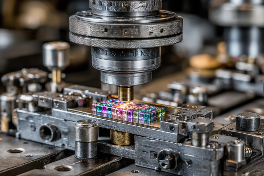
 Sputtering Target
 Tubes
Tubes
 Washer
 Wires
Wires
 Converters & Calculators
 Write for Us

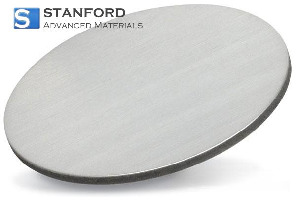
Custom Fe/Co Sputtering Targets for Precise Magnetic Thin Film Deposition in Spintronic Research

Customer Background
Our customer, a renowned research group based in Germany, is led by an experienced researcher focused on advancing the understanding of magnetic materials in spintronic device development. With a strong background in energy research, their work centers on achieving reliable magnetic properties essential for next-generation electronic applications. The team's experiments required a custom sputtering target to enable simultaneous deposition of Fe, Co, and Ni thin films via DC co-sputtering. Their previous experience with standard sputtering targets revealed inconsistencies in film uniformity and performance, particularly with composite magnetic systems. Facing these challenges, they approached us with detailed technical schematics and process requirements to tailor a solution conducive to their stringent specifications.
Challenge
The primary challenge was to design sputtering targets that allowed consistent and controlled deposition of magnetic films while handling the inherent difficulties of co-sputtering multiple magnetic elements. Specific technical and operational requirements included:
· Achieving a controlled ratio in the co-sputtering process of Fe, Co, and Ni with each metal's purity maintained at or above 99.95%.
· Maintaining precise target thickness and dimension tolerances: features such as a 12 mm thickness with a tolerance of ±0.02 mm and surface flatness below 0.1 microns were critical.
· Ensuring the target's structural integrity under DC sputtering conditions, which imposed the risk of film instability due to thermal fluctuations during continuous operation.
· Accommodating real-world constraints like lead time limitations due to synchronized experimental schedules and the necessity to integrate with existing deposition systems that were sensitive to target geometry and bonding interfaces.
The team had previously experienced sputtering inconsistencies such as drift in deposition rates, which resulted in non-uniform film thickness and unpredictable magnetic properties. Such issues led to repeated recalibrations and delays, highlighting the need for targets with enhanced thermal management and mechanical stability.
Why They Chose SAM
When the research team reached out, they were looking for a supplier with not only decades of experience in advanced materials but also the ability to quickly adapt to specialized and technical requirements. They chose Stanford Advanced Materials (SAM) because:
· Our track record of over 30 years in advanced material supply and our extensive inventory of over 10,000 materials gave them confidence in our capability to meet rigorous specifications.
· We provided early-stage engineering feedback, questioning initial design parameters such as the effects of thermal stress and the potential benefits of alternative bonding methods. This proactive consulting helped in redefining key design aspects.
· Our commitment to customized service allowed us to propose multiple configurations, including targets with both monolithic and hybrid bonding structures, to address potential issues related to heat dissipation and structural degradation during extended sputtering runs.
Solution Provided
At SAM, we took a comprehensive approach to develop a tailored solution. Our engineering team analyzed the full range of design drawings and process conditions provided by the customer. Key aspects of our solution included:
· Material Selection and Purity: We supplied Fe and Co with confirmed purities above 99.95% and integrated a carefully verified Ni additive for desired alloy characteristics in the co-sputtering process. The strict control of elemental purity minimized undesired impurities that could affect magnetic film properties.
· Dimensional and Surface Tolerances: The targets were machined with an overall thickness of 12 mm and a tolerance of ±0.02 mm to ensure compatibility with the existing clamping and deposition system. A surface flatness of less than 0.1 microns was achieved to facilitate uniform ion bombardment during sputtering.
· Bonding and Thermal Management: Recognizing the risk of thermal instability inherent to DC sputtering, we developed a dual configuration of targets. One configuration featured a monolithic target design while the other incorporated a copper-backed bonding layer. The copper backing improved thermal dissipation, reducing localized heating and subsequent film instabilities over prolonged sputtering cycles. The bonding interface was engineered with an optimized adhesive layer, maintaining dimensional stability and preventing delamination even with repeated thermal cycles.
· Packaging and Delivery: To address the tight lead time demands of the research schedule, we ensured each target was vacuum-sealed immediately after production. This precaution minimized oxidation and surface contamination, guaranteeing that the targets arrived in pristine condition ready for immediate integration into the co-sputtering system.
Results & Impact
After the integration of our custom targets, the research group documented several measurable improvements:
· Enhanced Film Uniformity: The improved target surface quality and optimized alloy composition led to a significant reduction in variances of film thickness across multiple deposition cycles, allowing the research team to achieve more consistent magnetic behavior.
· Improved Thermal Stability: The copper-backed configuration specifically demonstrated a notable improvement in heat dissipation, reducing thermal drift during prolonged DC sputtering cycles. This stability contributed to more reproducible deposition parameters and magnetic film performance.
· Process Efficiency: By mitigating variability in the sputtering process, the research group reported a reduction in recalibration downtime. This reliability allowed them to focus on experimental iterations rather than troubleshooting equipment inconsistencies, effectively streamlining the overall research progress.
The robust performance of both target configurations provided the team with actionable data for further refinement of their spintronic devices, affirming the value of our technical precision.
Key Takeaways
A successful sputtering process in magnetic material research demands not merely a high-purity material but a holistic approach that incorporates precise machining, reliable bonding, and effective thermal management. Our collaboration with the research team underscored several critical insights:
· Tailored material properties, achieved through stringent elemental purity and dimensional control, are essential for reproducible thin film deposition.
· Addressing thermal management early in the design phase can prevent deposition inconsistencies in DC co-sputtering operations.
· An experienced supplier capable of deep technical consultation, as demonstrated by Stanford Advanced Materials (SAM), is invaluable when navigating the complex interplay of material properties and deposition dynamics.
This case underscores that thoughtful engineering adjustments—not just the base material quality—are key to harnessing optimal performance in advanced magnetic thin film research.

 Dr. Samuel R. Matthews