Bars
Bars
 Beads & Spheres
 Bolts & Nuts
 Crucibles
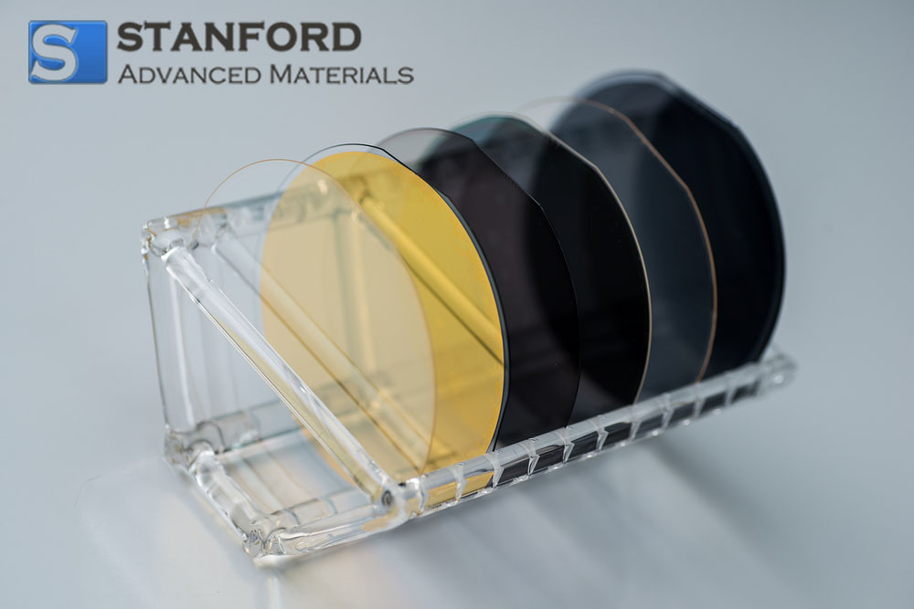
 Discs
Discs
 Fibers & Fabrics
 Films
Films
 Flake
Flake
 Foams
Foams
 Foil
Foil
 Granules
 Honeycombs
 Ink
Ink
 Laminate
 Lumps
Lumps
 Meshes
 Metallised Film
 Plate
Plate
 Powders
 Rod
Rod
 Single Crystals
 Sputtering Target
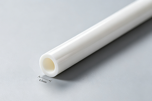
 Tubes
Tubes
 Washer
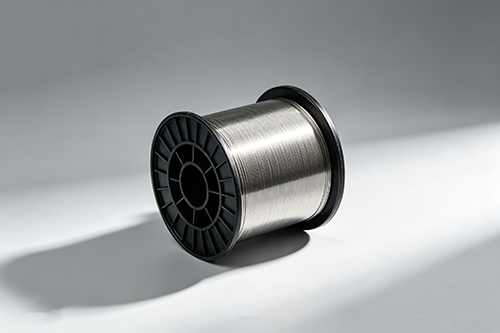
 Wires
Wires
 Converters & Calculators
 Write for Us

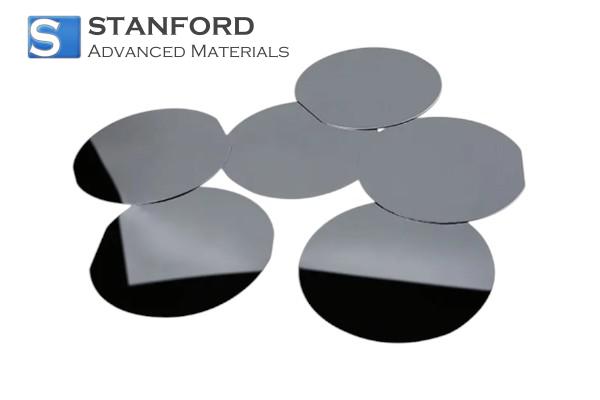
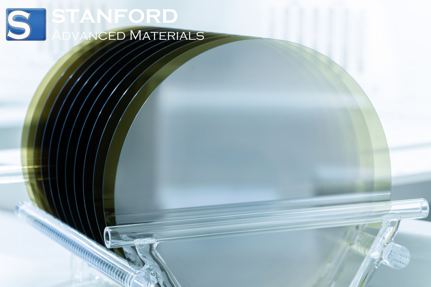
IR-Grade Germanium Wafer for Thermal Imaging Components in the Semiconductor and Optics Industry

Customer Background
Our client is a well-established manufacturer in the semiconductor and optics sector, specializing in thermal imaging systems and IR spectroscopy devices. With a longstanding presence in the European market, this company has continually refined their product performance to meet increasingly demanding technical standards. Their high-resolution imaging products rely significantly on the quality and consistency of IR optical components, where even minor deviations in material properties can affect operational reliability.
Facing escalating quality demands and a need to maintain stringent performance metrics, they reached out to us with detailed requirements. Their project called for an IR-grade germanium wafer, specifically engineered to serve as a substrate for infrared optical components. The design included tight specifications relating to material purity, wafer thickness, and dimensional tolerances essential for ensuring consistent imaging performance.
Challenge
The key challenge was twofold. First, the manufacturer required a germanium wafer with ultra-high purity (greater than 99.999%) to minimize impurities that could interfere with IR transmission. Second, the wafer needed to be dimensionally consistent, with a specified thickness of 500 µm (±2 µm) and a precise diameter of 100 mm (±0.1%). Such strict tolerances were necessary to ensure compatibility with their optical assembly processes, where even minimal variations could cause focal inconsistencies and signal instability.
Additionally, the client was operating under a tight schedule, with a lead time constraint that demanded expedited manufacturing and delivery of the wafers. Previous attempts with other suppliers resulted in delays and variabilities in quality, forcing them to seek a partner with a proven track record in high-precision material delivery and customization options.
Why They Chose SAM
After evaluating several potential supply partners, the client ultimately chose Stanford Advanced Materials (SAM) based on our extensive experience and our commitment to technical rigor. When they first presented their engineering drawings and detailed specifications, our team provided immediate technical feedback regarding several critical points:
· The impact of impurity levels on IR transmission, recommending a minimum purity level of 99.999%.
· Detailed recommendations on optimizing thickness tolerances to enhance compatibility with their optical system.
· Suggestions on packaging methods to mitigate the risk of micro-scratches and contamination during transport, thus preserving the wafer's surface quality.
Our proactive inquiries and tailored advice helped the client refine their requirements and served as a testament to our deep engineering expertise and commitment to precision. The customer appreciated the clear explanation of material characteristics and the realistic assessment of production capabilities—factors that solidified their decision to collaborate with us.
Solution Provided
At Stanford Advanced Materials (SAM), our team developed a comprehensive plan to meet the client's high demands for an IR-grade germanium wafer. The solution was engineered to address both the technical specifications and the real-world constraints highlighted by the client.
Key technical details included:
· Achieving a purity level of 99.999% in the germanium raw material, with rigorous quality control to avoid trace impurities that could degrade IR performance.
· Maintaining a wafer thickness of 500 µm with a precision tolerance of ±2 µm, ensuring consistent optical performance across the substrate.
· Providing a 100 mm diameter wafer with a tolerance of ±0.1%, crucial for proper alignment in the optical assembly process.
· Implementing advanced edge-finishing protocols to reduce chipping risks and to ensure that the wafer's active areas remained pristine.
In addition to the core material specifications, we addressed the client's logistical constraints by streamlining our manufacturing process. Real-world project requirements such as the lead time were tackled by prioritizing production scheduling and ensuring expedited shipping methods. Our packaging solution involved individually vacuum-sealed wafers housed in vibration-dampening carriers to eliminate any mechanical stress during transit. These measures ensured that the wafers reached the client in optimal condition, ready for integration into their imaging systems.
Results & Impact
Post-deployment, the client reported that the upgraded IR-grade germanium wafers significantly improved the overall performance of their optical components. The maintained purity level successfully minimized IR signal absorption interference, thereby ensuring high transmission efficiency. The precise thickness and diameter tolerances translated into better alignment with their optical apparatus, contributing to a consistent focal quality and reliable spectral performance.
In rigorous performance testing, the devices exhibited reduced signal variability and improved thermal imaging resolution. The predictable behavior of the wafer substrates minimized calibration issues, which in turn decreased the frequency of maintenance adjustments on the production line. Despite the challenges posed by the tight lead time, the client noted that our ability to expedite production and maintain quality was critical to keeping their project timeline on track.
Key Takeaways
The collaboration underscored several essential points for delivering advanced optical materials in high-spec environments:
· Adhering to ultra-high purity standards is critical when material performance is directly linked to system functionality. In this case, a purity threshold of 99.999% proved essential for achieving flawless IR transmission in optical components.
· Precise control over material dimensions, including thickness and diameter, is instrumental in ensuring compatibility with precise optical alignment systems, which can directly influence the quality of thermal imaging performance.
· Addressing real-world constraints such as tight lead times and transport-related stresses ensures that the material not only meets the technical requirements but also integrates seamlessly into the client's manufacturing workflow.
Through targeted technical expertise and a commitment to meeting challenging specifications, we at SAM demonstrated our capability to supply materials that genuinely meet demanding industrial needs while maintaining reliability despite logistical pressures.
 Dr. Samuel R. Matthews