Bars
Bars
 Beads & Spheres
 Bolts & Nuts
 Crucibles
 Discs
Discs
 Fibers & Fabrics
 Films
Films
 Flake
Flake
 Foams
Foams
 Foil
Foil
 Granules
 Honeycombs
 Ink
Ink
 Laminate
 Lumps
Lumps
 Meshes
 Metallised Film
 Plate
Plate
 Powders
 Rod
Rod
 Single Crystals
 Sputtering Target
 Tubes
Tubes
 Washer
 Wires
Wires
 Converters & Calculators
 Write for Us

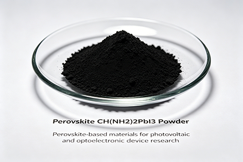
High-Purity Perovskite Powder Enables Accurate Photovoltaic Research

Customer Background
A leading research laboratory within the United States, specializing in chemical manufacturing and device development, required a precise volume of perovskite CH(NH2)2PbI3 powder for early-stage photovoltaic and optoelectronic experiments. The group had been working on optimizing thin-film deposition processes for solar cells and related devices, seeking improved material consistency to ensure repeatable experimental outcomes. Their previous material sources did not consistently meet the required control over purity and particle size, resulting in variability in device performance.
Challenge
The project presented several technical challenges. The research team required:
- A lab-scale quantity of 50 g to conduct feasibility experiments before scaling up.
- A perovskite powder with a purity of at least 99.9% to avoid interference from impurities during film deposition.
- Tight control over particle size distribution, with the target median value in the low-micrometer range, ensuring a predictable film formation process.
- Packaging under controlled atmospheric conditions, considering the moisture sensitivity of perovskite compounds.
- A delivery timeline compatible with an ongoing research schedule where delays might negatively affect device prototyping cycles.
Prior material supplied by other vendors had exhibited issues with storage-induced degradation and inconsistent particle sizing. These drawbacks interfered with achieving the desired electronic characteristics of the photovoltaic devices, as subtle inconsistencies in the raw material led to variations in film quality and device efficiency.
Why They Chose SAM
The research team opted for Stanford Advanced Materials (SAM) after a thorough technical review of potential suppliers. During initial consultations, our team provided candid feedback on several parameters:
- We directly addressed the need for high analytical-grade purity, confirming that the perovskite powder would meet or exceed 99.9% purity.
- Our engineers discussed particle size control, ensuring that our milling and processing techniques could maintain the target distribution with an acceptable deviation of less than ±5%.
- The importance of inert gas packaging to prevent degradation was acknowledged, and we detailed our packaging method designed to minimize exposure to moisture.
- A realistic lead time was proposed to synchronize with the lab's testing schedule, an assurance that few other suppliers could match given the customization required.
This technical dialogue reassured the research team that SAM not only understood the material requirements at a granular level but also could provide a solution that integrated well with their existing experimental protocols.
Solution Provided
SAM crafted a customized solution for the laboratory's perovskite needs. Key technical considerations addressed the challenges head-on:
- The supplied CH(NH2)2PbI3 powder was produced with a confirmed purity level of 99.9%, verified through high-resolution spectroscopic analysis.
- Particle size control was maintained using a refined milling process, yielding a median particle size of 3–5 µm with a +/– 5% tolerance, ensuring uniform dispersion during the film-coating process.
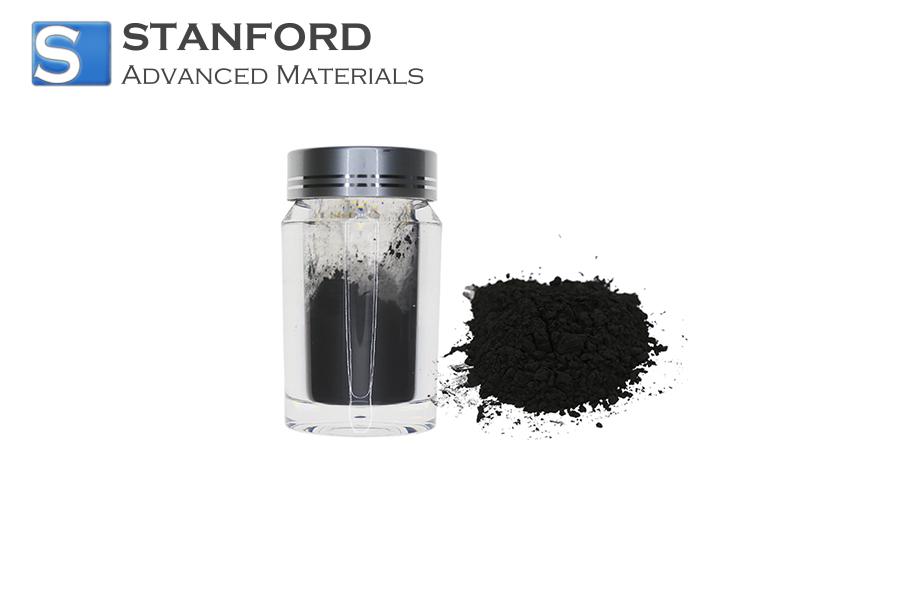
- Recognizing the instability of perovskite powders in ambient conditions, we packaged the 50 g sample in a vacuum-sealed container filled with high-purity nitrogen. This packaging design prevented moisture uptake and oxidation, preserving the integrity of the material.
- Each batch produced was subjected to rigorous quality control protocols, including X-ray diffraction (XRD) and scanning electron microscopy (SEM) analyses to verify phase purity and morphology.
- SAM's logistical support included confirmed shipment and storage guidance to align with the laboratory's narrow experimental time window, reducing the risk of material aging or degradation upon receipt.
Throughout the process, we maintained open technical communication with the customer, discussing iterative measurements and potential adjustments to meet evolving research requirements. This approach provided the necessary degree of customization critical for their advanced research.
Results & Impact
Upon receiving the perovskite powder, the research team integrated the material into their experimental setup with minimal adjustment. With the high-purity product and well-controlled particle size:
- They observed more consistent thin film deposition, which in turn led to improved uniformity in the photovoltaic layers.
- The inert packaging maintained material integrity throughout transit and storage, evidenced by a lower-than-expected incidence of moisture-induced defects.
- The controlled particle size contributed to reproducible film morphology, a factor that directly influenced device performance consistency across multiple test runs.
- The alignment of lead times with the critical phases of the research schedule meant that the experimental protocol proceeded without delay, contributing to smoother prototyping and testing cycles.
These outcomes allowed the laboratory team to progress in their research with greater confidence, ensuring that material-related variables did not undermine their investigation of new device architectures.
Key Takeaways
· Precision in material purity, particle size distribution, and packaging can have a significant impact on the development and testing of photovoltaic and optoelectronic devices.
· Detailed technical feedback and customization—as demonstrated by our work at Stanford Advanced Materials (SAM)—are essential to overcoming the inherent instability and sensitivity of advanced perovskite powders.
· Ensuring compatibility between material attributes and process requirements minimizes experimental variability, allowing research teams to focus on core device performance improvements.
· Close communication between the supplier and the research team, particularly in meeting tight lead time constraints and controlled environmental requirements, is pivotal for successful material integration.
The experience reinforces that well-defined technical specifications, when met with precise manufacturing and packaging protocols, translate into measurable improvements in experimental outcomes.
 Dr. Samuel R. Matthews