Bars
Bars
 Beads & Spheres
 Bolts & Nuts
 Crucibles
 Discs
Discs
 Fibers & Fabrics
 Films
Films
 Flake
Flake
 Foams
Foams
 Foil
Foil
 Granules
 Honeycombs
 Ink
Ink
 Laminate
 Lumps
Lumps
 Meshes
 Metallised Film
 Plate
Plate
 Powders
 Rod
Rod
 Single Crystals
 Sputtering Target
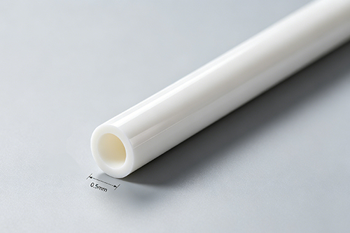
 Tubes
Tubes
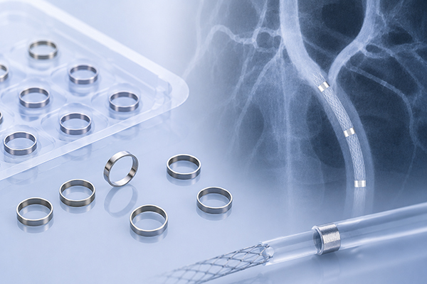
 Washer
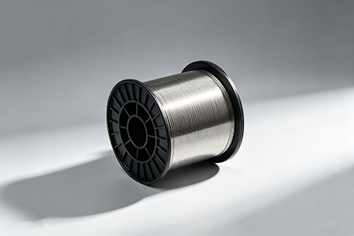
 Wires
Wires
 Converters & Calculators
 Write for Us

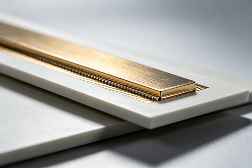
Robust ENEPIG-Coated AlN Substrates: Enhancing Thermal Management in Optical & Semiconductor Packaging

Customer Background
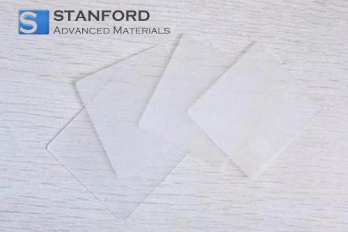
A prominent European manufacturer specializing in optical and semiconductor packaging was in need of advanced AlN substrates to support high-power die attachments. Their focus was on achieving efficient heat dispersion while ensuring a reliable soldering surface for delicate die components. With a rigorous production schedule and tight assembly tolerances, the team faced persistent challenges with conventional metallization processes. They had previously struggled with inconsistent plating quality and suboptimal adhesion, which led to occasional failures in die attachment during high-thermal load conditions.
Challenge
The manufacturer required aluminum nitride (AlN) substrates with a thermal conductivity exceeding 170 W/mK. Achieving the necessary performance meant addressing several technical and process constraints:
- The substrates needed a double-sided ENEPIG (electroless nickel, electroless palladium, immersion gold) coating. The coating had strict specifications: nickel layers between 3-7 µm, palladium layers between 0.1-0.5 µm, and gold layers between 0.05-0.1 µm.
- Uniformity was crucial. Variations in plating thickness or surface roughness, even minor, risked delamination during die attachment.
- Another focal point was ensuring high adhesion strength between the substrate and the plated layers. Inconsistent adhesion could lead to unstable solder joints once thermal cycling in operation began.
- There was also a tight turnaround constraint. The manufacturer needed a batch of 10 pieces processed under these exacting conditions with minimal lead time, as delays would affect production timelines.
Handling all these elements simultaneously was a non-trivial task. The plating process required precision control over deposition parameters while maintaining the high thermal conductivity inherent to the AlN ceramic.
Why They Chose SAM
Stanford Advanced Materials (SAM) entered the picture with over 30 years of experience and a proven ability to customize solutions for complex engineering challenges. Our global supply chain, managing over 10,000 materials and supporting more than 10,000 international customers, stood out as the ideal partner. During preliminary process discussions, we noticed subtle variances in the manufacturer's tolerance levels. By sharing these observations early on, our technical team helped recalibrate their design expectations before production, cutting down on the potential for trial-and-error later in the process.
The manufacturer also valued our technical depth when it came to metallization processes. Our prior work in semiconductor and optical materials assured them that our ENEPIG coating could meet their expectations for both uniformity and adhesion. In short, they needed a supplier who could deliver the rigor of quality control with a quick turnaround—a combination that SAM has delivered repeatedly.
Solution Provided
SAM addressed the challenge with a multi-faceted approach:
We started with the selection of premium AlN substrates that inherently provided a thermal conductivity greater than 170 W/mK. It was essential to confirm this property, as even the slightest deviation could impact die performance under operational loads. The substrates were then prepared for metallization in our clean-room environment to avoid any contamination.
The metallization process was carried out with close attention to each layer's thickness:
- Nickel Deposition: We applied a uniform nickel plating between 3 and 7 µm. This layer was pivotal, as it served as the foundation for the subsequent coatings.
- Palladium Layer: Next, a palladium deposition of 0.1 to 0.5 µm was closely monitored. We noticed during initial testing that even minor fluctuations in the palladium thickness could affect the final solderability.
- Gold Finish: Finally, the immersion gold was deposited at roughly 0.05-0.1 µm, ensuring excellent surface finish and primed solder bonding.

Each step was subjected to rigorous in-process inspections. We employed high-precision measurement systems to ensure coating thickness adherence within the defined ranges. Minor adjustments were made on-the-fly when our instrumentation indicated any slight deviations—often less than 0.02 µm—thus ensuring consistency across all ten pieces.
Surface characterization measurements confirmed minimal roughness levels. This control over surface texture was crucial, ensuring reliable die attachment without interference from micro-scale imperfections. Additionally, adhesion tests were performed to simulate thermal cycling, ensuring that the ENEPIG layers would remain firmly bonded during real-world operating conditions. During our process trials, we adjusted the plating parameters slightly to improve adhesion outcomes, leading to stable and robust performance under temperature fluctuations.
Packaging was the final step. Given the sensitivity of the plated surfaces, each substrate was carefully cleaned and packaged in a controlled environment. Labels indicating coating thicknesses and batch numbers were affixed for traceability, ensuring compliance with the manufacturer's strict quality assurance protocols.
Results & Impact
Following integration into the manufacturer's assembly line, the substrates provided several tangible benefits:
- The ENEPIG coating provided not only an excellent soldering surface but also maintained adherence even under repeated thermal cycling.
- Consistent thermal conductivity above 170 W/mK was maintained, ensuring that the heat generated from high-power semiconductor devices was effectively dissipated.
- The meticulous control over plating thickness directly translated to fewer instances of die attachment faults. This was evident in early production runs where corrective actions were minimal, thanks to our rigorous quality control checks.
- The reduced need for rework and lower scrap rates contributed to a more efficient assembly process and provided a noticeable reduction in production downtime.
Our technical team overall observed an improvement in reliability within the optical/semiconductor packaging process. The predictable performance of the substrates afforded design engineers better process stability—a key factor in high-volume production environments.
Key Takeaways
Precision in metallization is crucial when working with advanced ceramic substrates. By maintaining strict process controls and rigorous in-line measurement, we ensured that the ENEPIG coating met challenging technical specifications for both adhesion and surface quality. The case reinforces the significance of proactive engineering oversight along every step of the material processing workflow. Our experience at Stanford Advanced Materials (SAM) demonstrates that even small deviations in plating thickness or surface roughness can impact overall product performance.
The alignment of technical expertise with a responsive global supply chain allowed us to meet a demanding lead time while ensuring that every technical parameter was met. It is a reminder that attention to detail—combined with robust quality assurance—underpins reliable performance in demanding packaging applications.
In our engineering experience, working closely with customers to align on tolerances and process controls can be the difference between a successful production run and ongoing troubleshooting.
lyq8.jpg)
 Dr. Samuel R. Matthews