Bars
Bars
 Beads & Spheres
 Bolts & Nuts
 Crucibles
 Discs
Discs
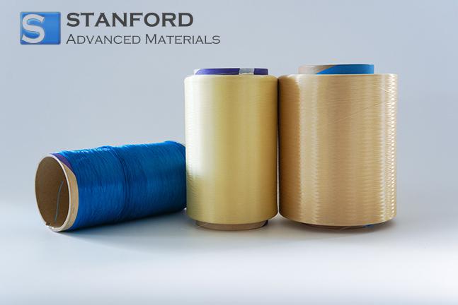
 Fibers & Fabrics
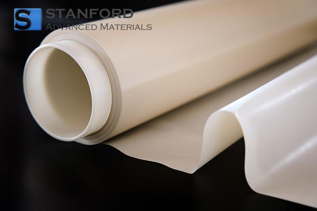
 Films
Films
 Flake
Flake
 Foams
Foams
 Foil
Foil
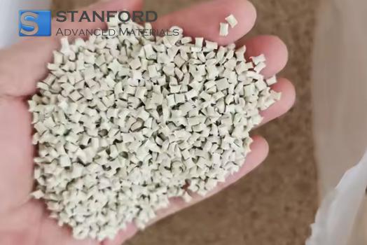
 Granules
 Honeycombs
 Ink
Ink
 Laminate
 Lumps
Lumps
 Meshes
 Metallised Film
 Plate
Plate
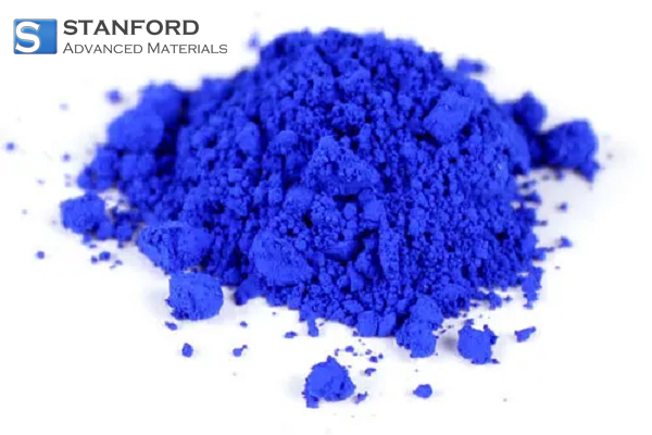
 Powders
 Rod
Rod
 Single Crystals
 Sputtering Target
 Tubes
Tubes
 Washer
 Wires
Wires
 Converters & Calculators
 Write for Us

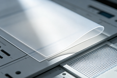
High-Uniformity LCP Films for Medical Substrate Integration in Electronics

Customer Background
A leading electronics supplier based in South Korea, known for its diverse portfolio, has been developing substrates for advanced medical devices. Their applications require films with exceptional dimensional stability, consistent dielectric performance, and verified biocompatibility. Their internal R&D team has been working on integrating LCP films into multi-layered device configurations. Although experienced in high-tech electronics manufacturing, they encountered difficulties sourcing LCP films that met medical-grade standards in both consistency and performance. Tight integration with their downstream processes meant that every micron of film uniformity was critical.
Challenge
Meeting the complex technical specifications was a significant hurdle. The customer needed LCP films available in 25 to 50 μm thickness that not only maintained high dimensional stability, but also exhibited a dielectric constant between 3.0 and 3.2 coupled with a dielectric loss factor (Df) of 0.002-0.005. The stringent tolerance for thickness uniformity was less than ±2 μm across the film width, a crucial factor to ensure that all devices performed predictably and consistently.
During early testing phases at the customer site, minor inconsistencies in thickness and dielectric properties were noted. This was worrisome since even slight deviations could lead to unpredictable electrode performance or signal loss. In practice, the project had an additional real-world constraint: a tight timeline. The supplier had to assure a consistent supply within a four-week window to avoid production delays in the customer's manufacturing cycle.
Why They Chose SAM
The customer selected Stanford Advanced Materials (SAM) because our decades-long experience—over 30 years in advanced material development and a catalog featuring more than 10,000 materials—was well-aligned with their rigorous technical requirements. They were particularly impressed by our ability to provide custom solutions, supported by our in-depth technical discussions and proactive approach in accommodating precise tolerances.
During initial meetings, our team noticed that the customer's tolerance requirement (±2 μm) was even stricter than what is standard in the industry for LCP films. This suggested that our technical advisors needed to focus meticulously on every processing parameter. Our responsiveness, backed by a global supply chain network, gave them the confidence that we could deliver the necessary specifications within the challenging lead time.
Solution Provided
SAM's approach was rooted in systematic process control and continuous improvement. Our solution involved several key measures:
1. Material calibration and formulation – We started by optimizing the polymer formulation to ensure that the base material offered inherent low dielectric losses. The LCP films were formulated to achieve a dielectric constant (Dk) in the narrow band of 3.0–3.2 while keeping the Df within 0.002–0.005.
2. Process adjustments for thickness control – To meet the critical 25–50 μm range with a uniformity tolerance of under ±2 μm, our processing equipment underwent fine calibrations. Each film batch was monitored in-line using high-resolution laser micrometers integrated into the production line. During initial tests, we noted slight variances at the film edges; minor adjustments in the extrusion die ensured uniform distribution of material throughout.
3. Strict quality control – SAM implemented a two-tier verification process. The first involved real-time monitoring of the film dimensions and dielectric properties during the coating process. The second was post-production laboratory testing using precision instruments to measure both film thickness and dielectric performance. Occasional deviations were immediately flagged, allowing for rapid adjustments to the process parameters, ensuring consistency across batches.
4. Customized technical support – Our engineering team maintained a close feedback loop with the customer. This collaborative effort included joint troubleshooting sessions and incremental refinements, such as thermal post-curing steps that further stabilized the dimensions. A particular observation during thermal cycling indicated that a slight modification in the heat profile reduced thickness variation, a finding that we adopted robustly across production batches.
5. Packaging and traceability – Every film roll was vacuum-sealed with proper moisture barriers and tagged with comprehensive technical data including exact thickness, dielectric metrics, and production batch details. This real-time traceability helped the customer validate film performance and ensured matching results with their device integration tests.
Results & Impact
The integration of SAM's LCP films resulted in a marked improvement in the reliability and efficiency of the customer's device substrates. Key observed outcomes included:
· Thickness Uniformity: Films consistently delivered within the 25–50 μm range, with uniformity maintained within the ±2 μm tolerance. This consistency significantly reduced the rework and calibration efforts on the customer's end.
· Dielectric Performance: All batches exhibited a tightly controlled dielectric profile (Dk 3.0–3.2 and Df 0.002–0.005) which, in turn, stabilized the electrical performance of the devices.
· Process Reliability: The tight turn-around of four weeks was maintained across multiple production cycles. Timely deliveries allowed the customer's manufacturing process to proceed without delay, thus avoiding costly downtimes.
· Enhanced Collaboration: Ongoing technical dialogue with our engineering team enabled the customer to tune their device assembly processes, especially during the integration of the LCP films into multi-layer configurations. This synergistic approach allowed them to achieve a smoother transition from prototype to production.
Our careful attention to technical detail and willingness to adjust process parameters on the fly was particularly appreciated. There were moments during production when minor variances were uncovered, but our immediate adjustments ensured continuous adherence to the high standards required.
Key Takeaways
Working with such strict tolerance levels—both in terms of physical dimensions and electrical properties—reinforced the idea that every micron counts in advanced materials engineering. The customer's experience highlights several important points:
· Customized technical support can mitigate real-world constraints such as stringent lead times and unpredictable process variations.
· In-line quality verification paired with post-production precision testing is essential in maintaining dimensional and dielectric property consistency.
· Collaborative, transparent dialogue between supplier and customer simplifies complex challenges and paves the way for rapid process refinements.
Stanford Advanced Materials (SAM) has proven that rigorous technical discipline and responsive engineering can create materials that reliably serve demanding applications, even under challenging manufacturing constraints. Our ongoing commitment to technical excellence means that we remain well-equipped to support advanced substrate applications in medical and electronic devices without sacrificing precision or quality.
 Dr. Samuel R. Matthews