Bars
Bars
 Beads & Spheres
 Bolts & Nuts
 Crucibles
 Discs
Discs
 Fibers & Fabrics
 Films
Films
 Flake
Flake
 Foams
Foams
 Foil
Foil
 Granules
 Honeycombs
 Ink
Ink
 Laminate
 Lumps
Lumps
 Meshes
 Metallised Film
 Plate
Plate
 Powders
 Rod
Rod
 Single Crystals
 Sputtering Target
 Tubes
Tubes
 Washer
 Wires
Wires
 Converters & Calculators
 Write for Us

High-Precision TiO2 Single Crystal Substrates for Optical Thin Film Deposition

Customer Background
A well-established, Germany-based optics firm specializing in electronic component manufacturing approached us with a unique requirement for ultra-precise single crystal TiO2 substrates. With decades of experience in crafting specialized optical components, their research and development team needed substrates for rigorous thin film deposition and extensive surface studies. They work primarily on prototyping nanostructured optical coatings and sensor arrays. Although their own facilities excel at deposition techniques, they needed an external supplier capable of reliably delivering substrates that adhere to extremely tight dimensional and purity specifications.
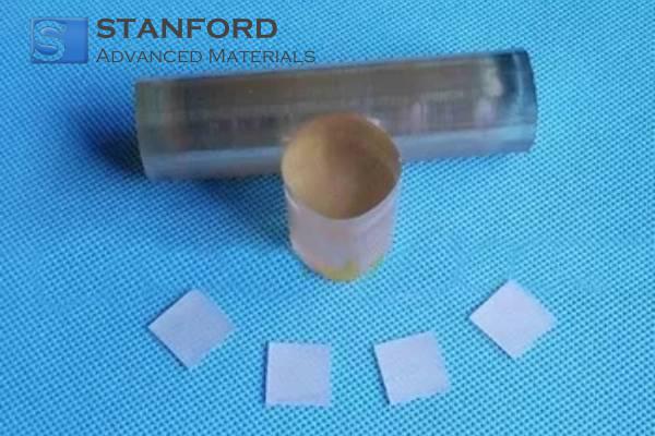
Their existing supplier had occasionally struggled to meet the stringent requirements of sub-millimeter tolerances and crystalline perfection. The customer emphasized that even minor surface disruptions or slight geometric variations could significantly disrupt the deposition process and subsequent device performance. The substrates, measuring 5 mm × 5 mm × 0.5 mm, were central to their experimental setups. Failure to maintain consistency across batches would inevitably lead to delays in their iterative fabrication processes.
Challenge
The customer's project presented multiple intertwined challenges:
· Dimensional Precision: Each substrate required precise dimensions of 5×5×0.5 mm with a tolerance of ±0.005 mm in thickness. Even a minute deviation could affect the optical and electrical properties of the final thin films.
· Surface Integrity: For optimal thin film performance, substrates needed an exceptional surface finish, with roughness less than 1 nm RMS. Any surface micro-defects could lead to non-uniform film deposition.
· Crystalline Perfection: The TiO2 single crystal substrates had to maintain excellent crystal orientation and a mosaic spread below 0.1°. Achieving this level of crystalline control repeatedly is inherently challenging.
· Packaging and Handling: Due to the substrates' critical nature, maintaining a contaminant-free environment during packaging was essential. They also required custom protective packaging that could prevent mechanical stress and environmental exposure during transit.
· Lead Time Constraints: The project timeline was tight. The customer needed the batches delivered promptly to match their experimental schedules, which demanded both manufacturing precision and efficient logistics.
Our team understood that any deviation could lead to experimental errors, increased costs, or even halt a vital research phase.
Why They Chose SAM
The customer selected Stanford Advanced Materials (SAM) due to our extensive track record in providing advanced materials solutions to global clients. Our 30+ years of experience and proven expertise handling over 10,000 materials made us a natural fit. Key reasons included:
· Technical Depth: Our long history of catering to precision-based industries meant that we were well-versed in meeting ultra-tight tolerances.
· Customization Ability: SAM quickly proposed solutions tailored to the detailed specifications – including enhanced surface polishing techniques and specialized packaging protocols – ensuring that the substrates would not suffer from mechanical or environmental degradation.
· Quality Assurance: The customer was reassured by our comprehensive in-line measurement techniques. For instance, during initial inspections, our team noted slightly variable thickness in prototype runs, and we immediately implemented tighter process controls.
· Global Supply Chain: Our efficient logistics network guaranteed that the production schedule would align with the customer's project timeline.
Solution Provided
Our engineers at Stanford Advanced Materials (SAM) collaborated closely with the customer's technical team to develop a robust, multi-step production plan that addressed each technical and logistical concern.
1. Material Selection & Preparation
We started by sourcing high-purity TiO2, with a purity level exceeding 99.95%, ensuring that any impurities did not interfere with the optical properties. The material underwent careful single crystal growth to maintain the requisite crystal orientation.
2. Precision Machining and Polishing
Using state-of-the-art CNC machining and precision lapping techniques, we crafted substrates to the exact dimensions of 5×5×0.5 mm. During initial testing, we noted minor deviations at the substrate edges; this observation led us to recalibrate our dicing machinery, achieving a final tolerance of ±0.005 mm.
The polishing process employed a multi-stage procedure, gradually reducing surface roughness to below 1 nm RMS. Our team found that a controlled, incremental polishing increased surface integrity and enhanced the substrate's suitability for subsequent thin film deposition.
3. Crystalline Quality Control
To ensure the crystalline perfection required, each substrate underwent X-ray diffraction (XRD) analysis confirming a mosaic spread below 0.1°. This step was critical for assuring that the film deposition would have a uniform nucleation surface, thus improving film adhesion and uniformity.
4. Custom Packaging
Recognizing that the substrates were susceptible to physical and environmental perturbations, we engineered a custom packaging solution. Each substrate was housed in a clean-room grade holder with shock-absorbing materials. Air is purged from the packaging and replaced with inert gas to guard against oxidation and particulate contamination during transit.
5. Quality Verification and Testing
Our quality control process involved repeated in-line measurement and verification steps. A laser interferometry system was used to measure substrate thickness, while surface roughness was continuously monitored with atomic force microscopy (AFM). Any substrate that did not meet the rigorous specifications was scrapped or processed further, ensuring batch uniformity.
Results & Impact
The customer witnessed a marked improvement in their thin film deposition processes following the integration of the SAM-supplied substrates:
· Consistent Dimensional Accuracy: The substrates consistently met the 5×5×0.5 mm specifications, with thickness variations strictly within ±0.005 mm. This precision meant that the deposition parameters remained stable across different batches, significantly reducing calibration intervals.
· Superior Surface Quality: The substrates exhibited a surface roughness reliably below 1 nm RMS, which translated to improved thin film uniformity. Early deposition trials showed fewer defects and better adhesion characteristics, enhancing overall device performance.
· Reliable Crystalline Structure: XRD results confirmed that each substrate maintained a mosaic spread of less than 0.1°. This level of consistency was crucial for achieving the observed uniformity in thin film properties.
· On-Time Delivery: Our efficient production and customized packaging solutions allowed us to adhere to the customer's strict timeline. This timely delivery ensured that their experimental schedules were maintained, avoiding costly delays.
During routine follow-ups, our team was pleased to hear that the improvements in substrate quality directly influenced the success of their subsequent trials. The close collaboration and openness during production adjustments allowed us to fine-tune the parameters effectively.
Key Takeaways
This project underscored the importance of having a supplier deeply familiar with ultra-precision manufacturing. Even marginal deviations in substrate dimensions or surface finish could seriously compromise thin film deposition processes. By focusing on rigorous quality assurance, from material selection through to final packaging, and by maintaining clear, technical communication with the customer, SAM was able to deliver solutions that met the demanding requirements.
Ultimately, the case highlights that when dealing with advanced optical materials, precision is paramount. Collaborative problem-solving and an uncompromising stance on quality control lead to material performance that supports robust, repeatable industrial processes. Our experience on this project reaffirmed the value of a meticulously engineered supply chain, ensuring that even the smallest components can have a substantial impact on a larger production system.
In the end, our team's hands-on involvement provided the customer with reliable, tailor-made substrates that not only met but exceeded their expectations, ultimately contributing to the seamless continuity of their research and production efforts.
 Dr. Samuel R. Matthews