Bars
Bars
 Beads & Spheres
 Bolts & Nuts
 Crucibles
 Discs
Discs
 Fibers & Fabrics
 Films
Films
 Flake
Flake
 Foams
Foams
 Foil
Foil
 Granules
 Honeycombs
 Ink
Ink
 Laminate
 Lumps
Lumps
 Meshes
 Metallised Film
 Plate
Plate
 Powders
 Rod
Rod
 Single Crystals
 Sputtering Target
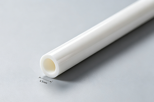
 Tubes
Tubes
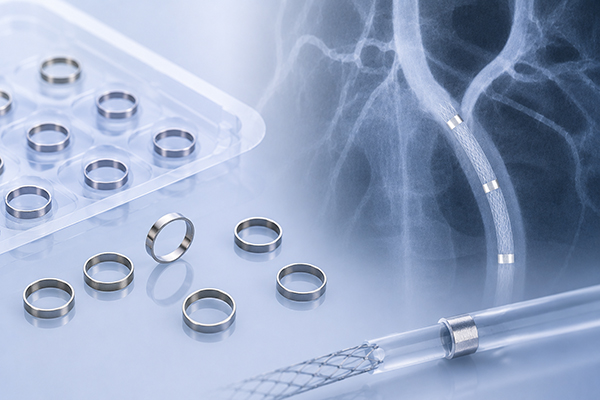
 Washer
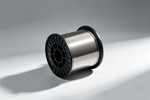
 Wires
Wires
 Converters & Calculators
 Write for Us

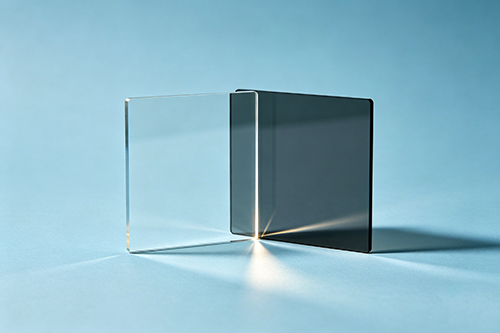
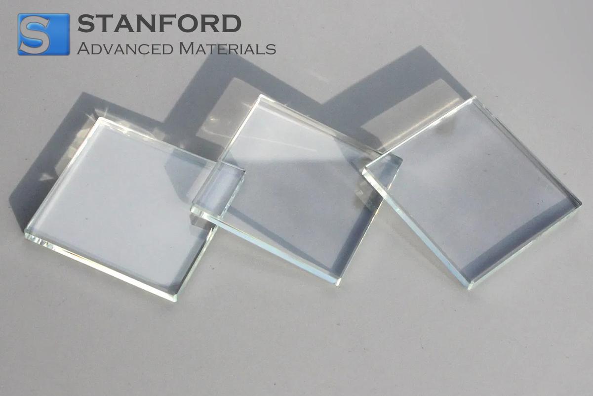
Ultra-Smooth BaF2 Crystal Substrates for High-Precision Photonic Applications

Customer Background
Our customer, a prominent semiconductor research organization based in the Netherlands, has a long history of exploring advanced photonic solutions. Their work centers on developing novel optical components that require exceptional clarity and minimal surface imperfections. With a focus on both optical and infrared applications, their projects demand substrates that consistently maintain sub-nanometer surface roughness. Although primarily a research entity, their rigorous testing and refined evaluation methods meant that even the slightest variability in material properties was subject to intense scrutiny.
Challenge
The team faced several intertwined challenges. The primary requirement was to secure barium fluoride (BaF2) crystal substrates with a surface roughness (Rq) lower than 1 nm—a threshold that left little room for error. The substrate needed to meet tight dimensional tolerances; for instance, the crystal thickness had to remain within ±0.02 mm of the specified 2.5 mm. Electrical compatibility with subsequent device coatings was also a factor, given that any surface irregularity beyond the sub-nanometer level could scatter light and impair device performance. A demanding lead time further compounded these issues. Previous attempts with off-the-shelf suppliers had resulted in inconsistencies mostly related to inadequate finishing processes and insufficient quality control on the optical surfaces.
Why They Chose SAM
The customer selected Stanford Advanced Materials (SAM) based on our proven track record. With over 30 years of experience and a library of more than 10,000 materials, SAM's expertise in custom substrate formulations was clear. Our global supply capabilities and history of working with diverse customer requirements reassured them that we could meet their tight tolerance and delivery timeline requirements. During early pilot evaluations, our team noted subtle deviations in surface finish metrics. Sharing those observations encouraged the customer to refine their acceptance criteria while aligning with our tailored processing methods, ultimately reducing the risk of downstream issues.
Solution Provided
Our approach began with a refined synthesis and stabilization process. We started by casting high-purity BaF2 crystals, ensuring that impurity levels remained below 99.9% to avoid any optical absorption anomalies. Once cast, the crystals underwent a multi-stage precision polishing sequence. Each polishing step was controlled in an environment with temperature stability maintained within ±0.5°C to ensure that thermal expansion did not introduce micro-scratches.
During the initial testing phase, we noticed slight variations in the polishing uniformity at the crystal edges. To address this, we adjusted the polishing pressure parameters—ensuring that the central areas and the periphery received an even finish. The surface roughness was then characterized using atomic force microscopy (AFM), verifying that Rq values consistently fell below 1 nm across the entire substrate.
In addition, we applied a controlled chemical etching process that eliminated sub-surface damage, a critical factor in maintaining the substrate's optical clarity. This process involved etching with a carefully formulated solution where the reaction time was strictly maintained at 45 seconds ±3 seconds to prevent over-etching. Every finished substrate was measured for key parameters: crystal orientation, thickness tolerance (±0.02 mm from the nominal value), and, importantly, verified for sub-1 nm surface roughness.
Packaging was another critical area. To prevent any contamination or surface damage during transit, substrates were vacuum-sealed in nitrogen-flushed packages, which also ensured moisture control.
Results & Impact
The collaboration yielded substrates that consistently met the stringent criteria set by the customer. The refined barium fluoride crystal substrates demonstrated an average surface roughness well below 1 nm—a benchmark rarely achieved with standard processes. The optical clarity and stability were such that subsequent deposition and coating stages encountered minimal scattering and interference.
Preliminary integration trials revealed that the substrates performed reliably under both optical and infrared testing. The compact package, combined with our in-line quality control systems, minimized variability and reduced waste. The customer noted fewer alignment issues during subsequent device assembly, confirming that our methodical approach was instrumental in streamlining their research prototypes.
Our team observed that even slight deviations—detected early through repeated AFM measurements—provided enough data to adjust parameters before full-scale processing. This adaptive process was essential in meeting the aggressive delivery deadlines. The efficient turnaround also allowed the customer to maintain their testing schedule without unforeseen interruptions.
Key Takeaways
Quality in advanced materials often comes down to attention to minute details. By maintaining a robust quality control system—measuring crystal thickness to within ±0.02 mm and ensuring sub-1 nm surface quality—we were able to produce BaF2 substrates that met demanding optical and infrared criteria. Our proactive adjustments during polishing and etching phases highlighted the importance of continuous process feedback.
Stanford Advanced Materials (SAM) continues to provide tailored solutions even in the most challenging applications. This case reinforces the value of precision engineering and strict process control. In the end, the true measure of success was the positive impact on the customer's product assembly, reducing both alignment issues and testing delays.
Each phase of our work, from material synthesis to final packaging, was a testament to our commitment to delivering reliability when it matters most.
 Dr. Samuel R. Matthews