Bars
Bars
 Beads & Spheres
 Bolts & Nuts
 Crucibles
 Discs
Discs
 Fibers & Fabrics
 Films
Films
 Flake
Flake
 Foams
Foams
 Foil
Foil
 Granules
 Honeycombs
 Ink
Ink
 Laminate
 Lumps
Lumps
 Meshes
 Metallised Film
 Plate
Plate
 Powders
 Rod
Rod
 Single Crystals
 Sputtering Target
 Tubes
Tubes
 Washer
 Wires
Wires
 Converters & Calculators
 Write for Us

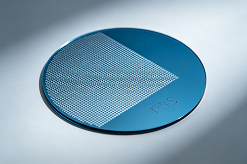
4-Inch Patterned Sapphire Substrate with Backside Laser Marking for Medical Optics Traceability

Customer Background
A medical optics developer was moving from bench-scale prototypes into a more structured wafer workflow. Their device architecture depended on 4-inch patterned sapphire substrates, and they needed the wafers to stay consistent across both small and larger pilot lots. The team was especially focused on traceability. Each wafer had to carry a readable backside mark so samples could be tracked through thinning, dicing, inspection, and assembly without confusion.
They were working under a fairly common constraint: multiple build stages, limited room for handling errors, and a deadline tied to validation testing. During early setup, our team learned that the customer wanted 100 wafers for immediate development and a second lot of 500 wafers once the process window was confirmed. That meant the supply had to support both short-run engineering work and follow-on production planning.
Challenge
The project had a few technical pressure points.
First, the patterned sapphire substrate geometry needed to stay consistent from wafer to wafer. The customer was concerned about pattern height, pitch uniformity, and edge-to-edge variation because even small deviations can affect optical behavior and downstream bonding results. They were targeting 4-inch wafers with a pattern profile that held within a tight process window, and they wanted the backside to remain suitable for laser marking without compromising handling quality.
Second, traceability had to survive the entire process flow. The mark needed to remain legible after cleaning, temporary bonding, backside processing, and inspection. That sounds straightforward, but sapphire is unforgiving when it comes to surface condition and marking contrast. If the laser energy is too aggressive, the backside can show localized damage or micro-fracturing. If it is too light, the code becomes unreliable under standard inspection lighting.
Third, the team needed a realistic lead time. Their internal schedule allowed little room for repeated sampling, and they were not looking for a generic wafer supply. They needed a supplier who could coordinate custom patterning, marking, and packaging in a way that reduced handling risk.
Why They Chose SAM
They selected Stanford Advanced Materials (SAM) because our team could support both the patterned sapphire substrate and the marking requirement in one workflow. That mattered. It reduced handoffs and kept the traceability process under one quality system.
We also had the production flexibility to handle two lot sizes, 100 wafers for immediate evaluation and 500 wafers for the next phase, without changing the material specification. Our global supply network helped keep the schedule realistic, and our technical team was able to discuss the backside marking method in practical terms rather than treating it as an afterthought.
During initial discussions, we noticed the customer was trying to balance mark depth against optical cleanliness. That suggested they had already seen how easy it is to over-process a sapphire backside. We recommended a controlled marking approach and aligned the wafer labeling format with their internal lot-tracking convention.
Solution Provided
SAM supplied 4-inch patterned sapphire substrates with custom surface patterning tailored to the customer's device flow. The substrate dimensions were held to a stable 4-inch format, and the pattern geometry was maintained across the lot using controlled fabrication checks. For a project like this, consistency mattered more than heroic tolerances. The wafers had to behave the same way in every run.
For traceability, we added backside laser marking with a non-intrusive process window. The mark was positioned on the rear surface so it would not interfere with the active-side optics or front-side processing. We kept the marking format compact and readable, and we confirmed that the code remained usable after standard handling steps. The customer specifically wanted identification that could survive sample routing through multiple stations, so we treated that as a packaging and process-control issue, not just a label request.
We also paid attention to packaging. The wafers were packed to limit surface contact and transport damage, with lot separation maintained between the 100-wafer pilot quantity and the 500-wafer follow-on order. Our team found that clear packaging segregation reduced operator mistakes during intake. Simple, but useful.
A few technical details guided the final supply:
- 4-inch patterned sapphire substrate format for prototype and pilot production
- Backside laser marking for wafer-level identification and lot traceability
- Surface consistency checks to maintain pattern geometry across batches
- Protective packaging to reduce edge chipping and contamination during shipment
- Lot-separated labeling to support the customer's internal QA workflow
Results & Impact
The customer received wafers that fit both the development phase and the next procurement stage without changing their internal handling process. The backside markings were readable during inspection and remained useful through downstream routing. That reduced manual transcription and the kind of labeling confusion that tends to show up once multiple engineers start touching the same wafer stack.
More importantly, the patterned sapphire substrates arrived with the consistency the customer needed to continue device testing. The team reported fewer questions during incoming inspection, and the wafers moved through their setup without additional sorting or rework. During early testing, we noticed the customer was especially sensitive to handling damage at the edges; the packaging approach helped there, and that was reflected in their acceptance review.
The dual-quantity structure also helped them plan ahead. The 100-wafer lot supported immediate trials, while the 500-wafer inquiry gave them a path toward scaling once the process was locked. That kind of continuity matters in optical and medical device programs. Delays usually come from small mismatches between prototype materials and production materials, not from the big milestones.
Key Takeaways
This project came down to control and traceability. Patterned sapphire substrates need stable geometry, and when the wafers are used in medical optical development, backside identification becomes part of the process discipline. A readable laser mark is not just a convenience. It can keep a pilot line from losing track of sample history.
Stanford Advanced Materials (SAM) was able to support the substrate, the marking, and the packaging as one coordinated supply, which helped the customer move from test planning into practical wafer evaluation. For teams working with sapphire-based optical devices, that combination is often what prevents small documentation issues from becoming process delays.

 Dr. Samuel R. Matthews