Bars
Bars
 Beads & Spheres
 Bolts & Nuts
 Crucibles
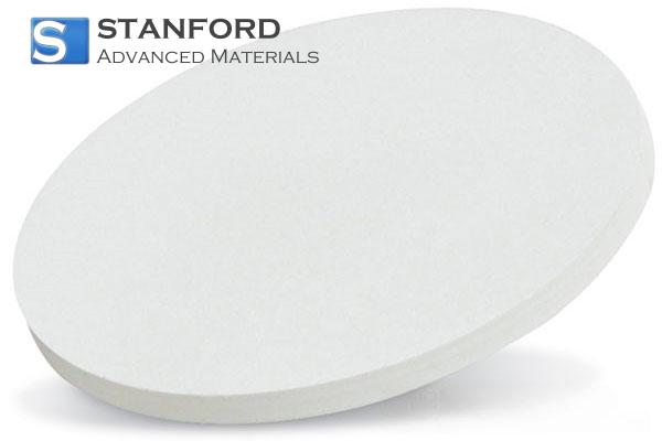
 Discs
Discs
 Fibers & Fabrics
 Films
Films
 Flake
Flake
 Foams
Foams
 Foil
Foil
 Granules
 Honeycombs
 Ink
Ink
 Laminate
 Lumps
Lumps
 Meshes
 Metallised Film
 Plate
Plate
 Powders
 Rod
Rod
 Single Crystals
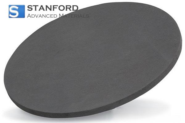
 Sputtering Target
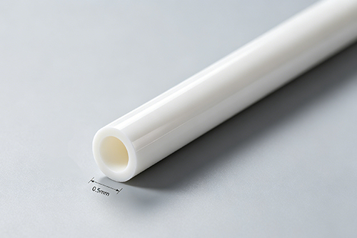
 Tubes
Tubes
 Washer
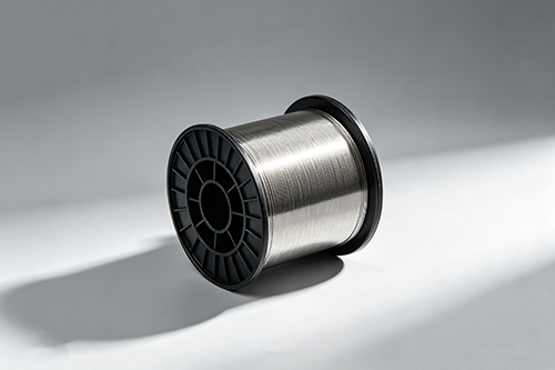
 Wires
Wires
 Converters & Calculators
 Write for Us

Custom NbN/AlN Multilayer Sputtering Target for Superconducting and Piezoelectric Device Research

Customer Background
A prominent research laboratory at a well-established Asian university has been engaged in the development of superconducting and piezoelectric devices. Their experimental setups require highly controlled deposition of multilayer films on SiO₂ substrates. The research team had been using conventional sputtering targets but faced variability in film properties during extended sputtering runs. Their interest centered on employing multilayer targets composed of NbN and AlN to achieve the desired electrical and mechanical characteristics in the devices.
The team provided detailed deposition parameters and design drawings, specifying the need for a custom configuration of NbN and AlN layers. They required the targets to suit their RF magnetron sputtering process, which demanded high purity and strict dimensional tolerances. In addition, the team aimed to study the superconducting properties of NbN layers coupled with the piezoelectric behavior of AlN, a combination that posed significant technical challenges.

Challenge
The primary challenge lay in producing a sputtering target that offered consistent performance across multiple layers while staying within narrow technical tolerances. Key requirements included:
· NbN purity of at least 99.9% and AlN refined to a similar high purity, ensuring no contaminants interfered with electrical properties.
· Precise layer thickness control: the NbN and AlN layers had to be deposited with thickness deviations maintained below ±2%, as even minor variations could lead to considerable shifts in superconducting transition temperatures or piezoelectric constants.
· A design that allowed for efficient heat distribution during RF magnetron sputtering, thereby reducing the risk of thermal instability.
· Compatibility with existing sputtering systems where film uniformity over a 150 mm diameter target area was critical.
· A production timeline that required a turnaround within 4–6 weeks to coincide with the research agenda's scheduled experiments.
Past production runs with standard targets resulted in film instabilities, including non-uniform layer deposition and gradual performance degradation over time. The multilayer structure also imposed additional constraints on bonding between NbN and AlN layers, where mismatches in thermal expansion and bonding strength could negatively influence the sputtering process.
Why They Chose SAM
The research team evaluated several suppliers and eventually opted for Stanford Advanced Materials (SAM) due to our extensive technical expertise and track record in serving complex deposition requirements. Our team reviewed the provided design drawings in detail and engaged with the researchers on the potential impacts of thermal cycling and sputtering-induced stress on the multilayer structure. This early dialogue was crucial in refining the project's specifications.
Our responsiveness and hands-on approach gave the team confidence that SAM could deliver targets that met both the material purity and the dimensional control needed for a stable sputtering process. The capability to customize sputtering targets—and our familiarity with the technical intricacies of NbN/AlN multilayer systems—were decisive factors in their choice of SAM.
Solution Provided
At Stanford Advanced Materials (SAM), our team formulated a custom solution designed to address the multilayer sputtering requirements. The solution involved several technical considerations:
1. Material Purity and Physical Properties:
We sourced NbN and AlN materials with purities exceeding 99.9%, while controlling grain structure to achieve low internal stress. This helped reduce variability in sputtering yield and ensured electrical and mechanical consistency in the deposited films.
2. Layer Structuring and Tolerances:
Using advanced machining and layering techniques, we produced targets where the NbN and AlN were arranged in an alternating multilayer format. The target's overall dimensions were maintained within a tolerance of ±0.5 mm over a 150 mm diameter area. Additionally, each individual layer's thickness was controlled to within ±2% of the design specification, ensuring stable superconducting and piezoelectric properties.
3. Bonding and Thermal Management:
Given the thermal stresses associated with RF magnetron sputtering, the bonding interface between NbN and AlN layers was engineered for enhanced adhesion. A specially formulated interlayer bonding compound with high thermal conductivity was employed, which mitigated delamination risks during repetitive thermal cycling. The final assembly was also optimized for improved heat transfer, thereby aiding in the control of sputter-induced heating.
Furthermore, the targets were packaged in a controlled environment to prevent surface oxidation or contamination during transit. The packaging procedure included vacuum sealing and careful cushioning to prevent mechanical impacts that could disturb the precise edge tolerances critical for mounting in the sputtering system.
Results & Impact
Through extensive testing, the research team confirmed that the custom multilayer targets produced by SAM delivered consistent sputtering characteristics under extended operation. Key observed improvements were:
· Enhanced film uniformity across substrate areas, attributed to the carefully controlled multilayer structuring and optimized thermal management.
· Consistent superconducting transition temperatures and piezoelectric responses, indicating that the precise control over layer thickness and purity effectively minimized performance variability.
· A significant reduction in sputter-induced erosion and thermal instability, which previously led to deviations in film properties during multiple deposition cycles.
These improvements allowed the research team to focus on optimizing device performance rather than investing additional time and resources in addressing material inconsistencies. Although the targets still required minor adjustments in deposition parameters, the baseline performance was sufficiently stable to support detailed experimental investigations.
Key Takeaways
This case study illustrates the importance of precise material specifications and customized engineering in advanced thin film deposition processes. For demanding applications like superconducting and piezoelectric device research, even slight deviations in purity, bonding, and dimensional accuracy can have a pronounced effect on film performance. Selecting a supplier capable of detailed technical engagement and customization, as demonstrated by SAM, helps to ensure that the produced materials align closely with the experimental requirements. The experience reinforces that a collaborative, technically focused approach is essential when addressing real-world constraints in advanced material applications.
 Dr. Samuel R. Matthews