Bars
Bars
 Beads & Spheres
 Bolts & Nuts
 Crucibles
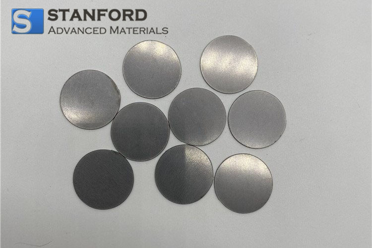
 Discs
Discs
 Fibers & Fabrics
 Films
Films
 Flake
Flake
 Foams
Foams
 Foil
Foil
 Granules
 Honeycombs
 Ink
Ink
 Laminate
 Lumps
Lumps
 Meshes
 Metallised Film
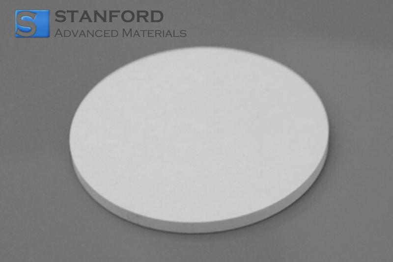
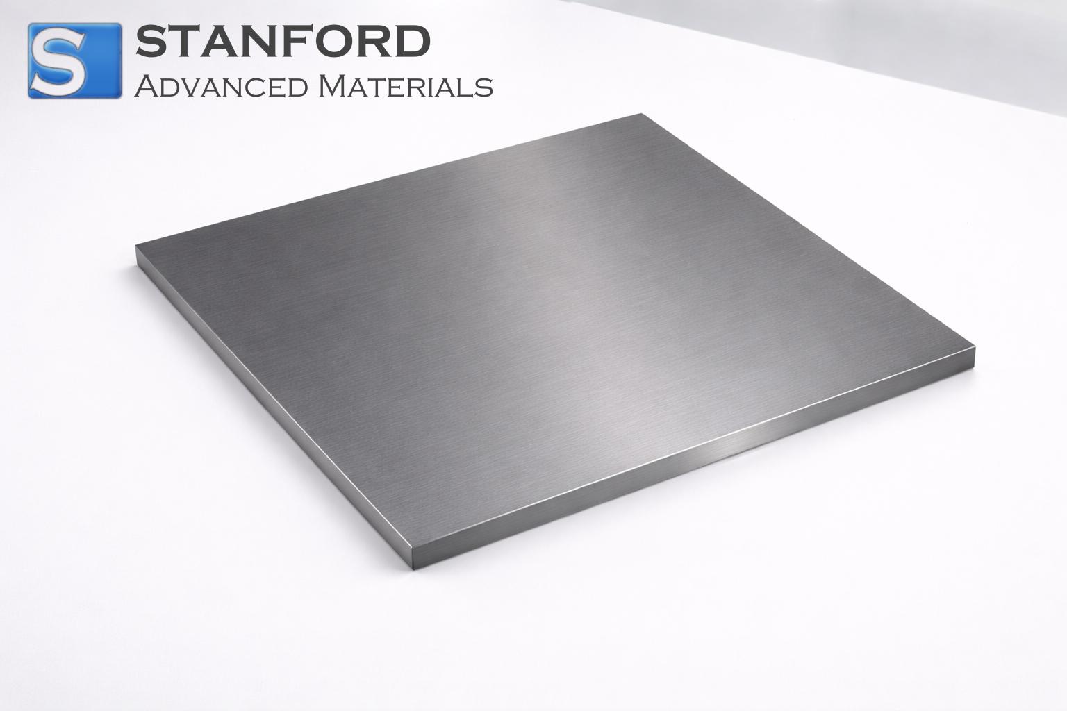
 Plate
Plate
 Powders
 Rod
Rod
 Single Crystals
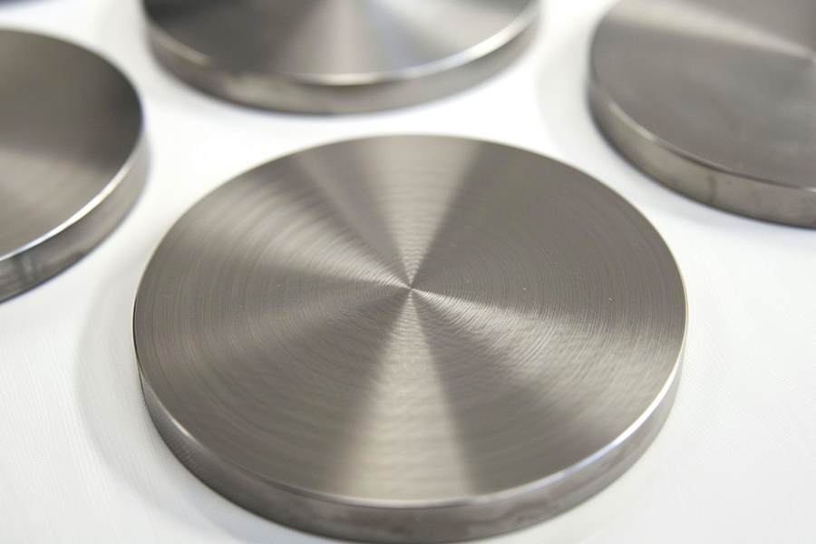
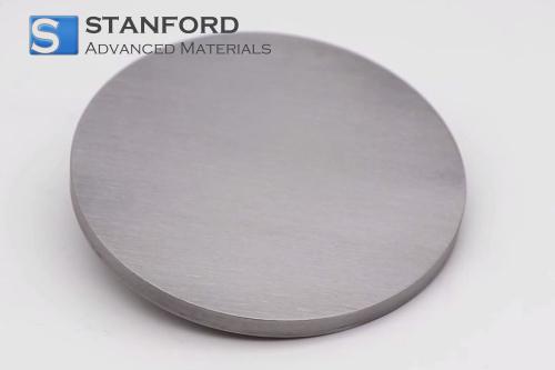
 Sputtering Target
 Tubes
Tubes
 Washer
 Wires
Wires
 Converters & Calculators
 Write for Us

How to Use Tantalum Sputtering Targets for Semiconductor Coatings

Tantalum's role in semiconductor manufacturing dates back decades, but what's changed is the precision required for its delivery. As chips shrink below 5nm and wafer sizes move to 300mm, the margin for error in sputtering targets has effectively vanished. A slight variation in grain size or a few ppm of impurities can render an entire batch unusable.
This is where tantalum targets come in—not just as raw material, but as engineered components. Whether you're running barrier layers for copper interconnects or building capacitor films for DRAM, the target specifications must match your process exactly. And increasingly, "exactly" means custom.
1. Sputtering Process Overview
Tantalum targets sit at the heart of physical vapor deposition (PVD) systems. Inside a vacuum chamber, ionized argon gas bombards the target surface, knocking off tantalum atoms that then travel to the substrate and condense into a thin film. The math is straightforward: deposition rates typically range from 1 nm/s under DC or RF power, and film thickness must remain within a few percent across the entire wafer.
What complicates the math is the target itself. A target with an inconsistent grain structure will eject atoms unevenly. A target bonded poorly to its backing plate can overheat and warp. This is why target manufacturers who treat sputtering as a commodity business miss the point—the target defines the film.
2. What Tantalum Does Inside a Chip
In production today, tantalum films serve two main functions:
- Barrier layers in copper interconnects: Copper diffuses readily into silicon and silicon dioxide, shorting out transistors. A 20–200 nm tantalum layer blocks that migration while maintaining low electrical resistance.
- Dielectric films in high-density capacitors: Tantalum's stable oxide (Ta₂O₅) provides the dielectric properties needed for DRAM and certain analog chips.
Both applications demand films with zero pinholes, consistent step coverage, and long-term stability under electrical stress. You can't get that from an off-the-shelf target that wasn't designed for your specific chamber geometry and power settings.
3. Why Target Specs Matter More Than You Think
Tantalum's physical properties are well known: melting point above 3000 °C, excellent corrosion resistance, and the ability to form dense, amorphous films. But here's what datasheets don't tell you:
The same tantalum can behave completely differently depending on how the target was processed. Grain orientation, oxygen content, and even the way the target was machined affect sputter behavior. For high-volume manufacturing, consistency from target to target matters as much as absolute purity.
That's where customization enters the picture. Running a production line means locking in parameters and never having to requalify a new target batch. If your process calls for a specific grain size to minimize particle generation, we can deliver that. If your chamber requires a particular backplate thickness to maintain cooling efficiency, that's on the table too.
4. What Customization Actually Looks Like
"Custom" in the context of tantalum sputtering targets covers a lot of ground:
-
Composition: Beyond pure tantalum, some applications need tantalum alloys—tungsten-tantalum, titanium-tantalum, or others—in precise ratios.
-
Purity and microstructure: From 3N5 to 5N and above, with controlled grain size and crystallographic texture to match your sputter tool's magnetic field configuration.
-
Physical dimensions: Targets can be circular, rectangular, or irregular shapes. Diameters vary from small R&D sizes up to large formats for 300mm wafer production.
-
Backplate integration: We supply monolithic targets or bonded assemblies with copper, molybdenum, or other backing materials, depending on your thermal management requirements.
The goal is simple: the target arrives ready to install and perform to your existing qualification standards. No process tweaking. No surprises.
5. Results You Can Expect
When the target matches the process, the results show up in production data:
-
Lower defect densities from reduced arcing and particle generation
-
Tighter thickness uniformity across the wafer
-
Longer target life, which means fewer chamber openings and less downtime
-
Repeatable film properties batch after batch
Chipmakers using properly matched tantalum targets report more stable yields and fewer excursions over long production runs. For capacitor applications, the electrical performance—leakage current, breakdown voltage, stability under bias—stays within spec without constant adjustment.
Conclusion
Tantalum sputtering targets aren't a commodity. They're a process parameter that happens to arrive in a box. Getting them right means understanding not just the material, but how it will be used—the chamber, the power levels, the film requirements, and the production environment.
We build targets to fit that picture, not the other way around. If you're qualifying a new process or looking to stabilize an existing one, we can put together a target specification that matches your exact needs. Contact us to discuss your application or request a quote with your target dimensions.
Frequently Asked Questions
Q: What purity levels are available for tantalum sputtering targets?
A: We supply purities ranging from 3N5 (99.95%) to 5N (99.999%) and above, depending on your application. Higher purities are typically specified for advanced nodes where metal contamination must be minimized.
Q: Can you match existing target dimensions from other suppliers?
A: Yes. If you're requalifying a second source or replacing an incumbent, we can manufacture to your exact mechanical drawings, including bolt patterns, counterbores, and backplate specifications.
Q: How does grain size affect sputtering performance?
A: Grain size and orientation influence the target's erosion profile and arcing tendency. Fine, randomly oriented grains generally provide more stable sputtering, especially in DC magnetron systems. We can tailor the microstructure based on your process.
Q: What backing plate materials do you offer?
A: Common options include copper, molybdenum, and various copper alloys. We also provide diffusion-bonded assemblies for high-power applications where thermal conductivity is critical.
Q: How do I determine the right target specs for my process?
A: Start with your film requirements—thickness, uniformity, resistivity—and work backward. We can help with recommendations based on similar applications or work with you to develop a custom specification.
 Chin Trento