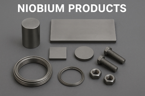
Bars
Bars
 Beads & Spheres
 Bolts & Nuts
 Crucibles
 Discs
Discs
 Fibers & Fabrics
 Films
Films
 Flake
Flake
 Foams
Foams
 Foil
Foil
 Granules
 Honeycombs
 Ink
Ink
 Laminate
 Lumps
Lumps
 Meshes
 Metallised Film
 Plate
Plate
 Powders
 Rod
Rod
 Single Crystals
 Sputtering Target
 Tubes
Tubes
 Washer
 Wires
Wires
 Converters & Calculators
 Write for Us

Niobium Applications in Electronics and Optics

Niobium is a very useful metal. In electronics, niobium helps in storing energy, facilitates superconducting systems, and improves the performance of semiconductors. In optics, it supports devices that change color, amplify light, and produce high-quality laser beams.
Niobium in Electronic Applications
1. Capacitors and Energy Storage
Niobium oxide capacitors have the capability of storing high energy density. Nibium capacitors are utilized in computers and mobiles. They discharge and charge energy with a high rate. In the majority of cases, they offer longer working time than other capacitors. This aspect makes them widely sought after in the field of consumer electronics.
2. Superconducting Electronics
Niobium is a superconducting structural material for superconducting electronics. Superconducting devices are always in very low temperatures. The superconducting nature of niobium reduces power loss. Some sensitive devices find these characteristics useful. Communication network filters, for instance, utilize niobium superconducting circuitry. Lossless and stable transmission is a giant advantage in high-speed data systems.
Further reading: Types of Superconducting Materials and Their Applications
3. Semiconductors and Thin Films
Niobium thin films are utilized by the majority of modern semiconductors for added performance. Thickness in such configurations is controlled to a few nanometers. This ensures proper operation in devices like sensors and integrated circuits. The thin films promote the adhesion and structural integrity of the semiconductor layers. Niobium is widely used in microchip fabrication to facilitate electron flow.
4. Sputtering Targets and Physical Vapor Deposition Applications
Niobium sputtering targets are used in physical vapor deposition processes. In use in such processes, niobium is bombarded with ions to produce a vapor that condenses to form thin layers on substrates. The process is useful when the production of hard coatings on glass and silicon wafers is desired. The process is common during the manufacture of modern-day electronic devices as well as during the production of reflective coatings in optical devices.
Niobium in Optical Applications
Niobium has earned recognition in the optical field. On account of its properties, it is the most suitable material for the greater part of the optical devices. I have noticed that it is being used to manufacture devices that demand accuracy and durability.
1. Electrochromic and Photochromic Devices
In materials where color and light are required to vary dynamically, niobium oxide is employed. The metal oxide reacts to electricity signals or light inputs, quickly and safely altering color. Dynamic lenses and intelligent windows belong to this group. The operation of niobium in these devices ensures rapid action and prolonged use.
2. Optical Coatings
Niobium coatings on optical coatings help in the control of reflection and light absorption. Niobium coatings are used on solar panels and camera lenses. They are glare-reducing agents as well as protectants for the material underneath. In most cases, a thin layer of niobium oxide extends the life of the device by serving as a protective shield against adverse environmental factors.
3. Laser and Photonic Components
Therefore, niobium is among the materials applied because of its improved heat and electrical conductivity in most laser technology. It is found in photonic components and cavities. In fiber optics, niobium is applied in thin films to enhance the transmission of signals with clarity and speed. Therefore, beam quality is maintained with reduced light loss by using niobium.
4. TCOs
Niobium transparent conductive oxides are gradually being applied in touch screens and display screens. They are electrically conductive and optically transparent. They can handle high resolution and stress. The stability of the smartphone and computer monitor is improved by applying niobium in TCOs.
Conclusion
Niobium is an essential component in electronics and optics. Its mechanical strength, high melting point, and its superconducting nature make niobium a superior material for high-end applications.
Frequently Asked Questions
F: In what way does niobium contribute to the improvement of capacitor performance?
Q: Niobium oxide capacitors provide high energy density and rapid release of energy, leading to better and stable device operation.
F: What benefits does niobium thin films offer in semiconductors?
Q: Niobium thin films facilitate electron conductivity, bonding, and reliability in microchips and sensor devices.
F: Why is niobium widely used in optical coatings?
Q: Niobium maximizes light control, reduces glare, and protects underlying materials in many optical components.
 Chin Trento