Bars
Bars
 Beads & Spheres
 Bolts & Nuts
 Crucibles
 Discs
Discs
 Fibers & Fabrics
 Films
Films
 Flake
Flake
 Foams
Foams
 Foil
Foil
 Granules
 Honeycombs
 Ink
Ink
 Laminate
 Lumps
Lumps
 Meshes
 Metallised Film
 Plate
Plate
 Powders
 Rod
Rod
 Single Crystals
 Sputtering Target
 Tubes
Tubes
 Washer
 Wires
Wires
 Converters & Calculators
 Write for Us

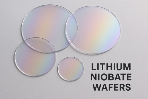
Lithium Niobate Wafers: A Detailed Review

What Is Lithium Niobate and Why It Matters
Lithium niobate is a compound of lithium, niobium, and oxygen. It has the formula LiNbO3. Lithium niobate exhibits great piezoelectric and optical properties. It is used in wearables, sensors, and light modulators by such properties. Lithium niobate wafers are employed in most optical modulators. Its use extends to telecommunications and defense. The material is depended upon in laboratories for studies and factories for production.
In simple terms, lithium niobate allows faster and more efficient control over sound and light in equipment. It's renowned among engineers and researchers for being reliable.
Main Physical and Chemical Properties
Lithium niobate is a solid substance. Its crystal structure has a high refractive index. For instance, the refractive index can be around 2.2 at normal wavelengths. It has high nonlinear optical coefficients as well. This means light signals can be switched on and off and altered effectively. The material is pyroelectric. This helps in sensing changes in temperature. Lithium niobate is chemically stable in a majority of environments. It keeps up well when used for extended times in equipment. It possesses a normal melting point of more than 1250°C. Its hardness and chemical stability are factors that make it long-lasting. It is commonly utilized in optical waveguides where there is a need for reliability in functioning. Researchers indicate that the large electro-optic effect of lithium niobate makes it perfect for state-of-the-art remote sensing equipment.
Types of Lithium Niobate Wafers
Lithium niobate wafers come in different forms. They vary with thickness and orientation. There is the single-crystal lithium niobate wafer that is most common. They are cut along various crystal axes. For example, X-cut and Z-cut wafers change the interaction of light with the material. There are wafers that have dopants. The dopants improve optical damage resistance. All types of wafers find application in other uses. Z-cut wafers are applied in research labs in second harmonic generation. Other uses apply X-cut wafers in high-speed data devices. The type allows engineers to choose the right wafer for each purpose.
Applications in Electronics, Optics, and Photonics
Applications for lithium niobate wafers are electronics, optics, and photonics. They take a pivotal part in modulators that control laser beams. Telecommunication networks, for instance, use these wafers in controlling high-speed signals. Photonic devices use them to guide and redirect light. In optical devices, the material's strong nonlinear properties prove useful. Most optical switches in fiber optic networks rely on lithium niobate. In electronic circuits, its piezoelectric nature makes it a precise sensor. This is utilized in sonar and ultrasonic imaging devices. The material is also used extensively in frequency doublers as well as in wavelength converters. A phase modulator used in the protection of guards in secure systems is an example. These examples show how lithium niobate wafers play an important part in modern technology.
Advantages over Other Materials
Lithium niobate wafers provide many benefits compared to other materials. The materials are stable and reliable for extended use. Their optical nonlinearity is several times higher than for most glasses or ceramics. This makes the devices more efficient frequency converters and signal modulators. The wafers operate effectively under various shifts in temperature. They are extremely robust. The material radiates high transparency of signal in fiber optic. In mechanical terms, lithium niobate is precise and deterministic. Industries consider it to be cheap relative to other rare or otherwise complex compounds. For exact applications, these wafers are typically the optimum choice.
Further reading: Lithium Tantalate vs. Lithium Niobate Wafers
Conclusion
Lithium niobate wafers are an important part of today's high-tech world. Their multifaceted properties suit them for various applications in electronics, optics, and photonics. Experts and engineers appreciate lithium niobate because of its strong performance and longevity.
Frequently Asked Questions
F: What is the chemical formula for lithium niobate?
Q: Lithium niobate is composed of the formula LiNbO3.
F: What is the main property that makes lithium niobate attractive in optics?
Q: Due to its high nonlinear optical coefficient, it can effectively modulate light.
F: Why are different wafer cuts important?
Q: Different cuts alter optical interaction and enhance performance in some applications.
 Chin Trento