Bars
Bars
 Beads & Spheres
 Bolts & Nuts
 Crucibles
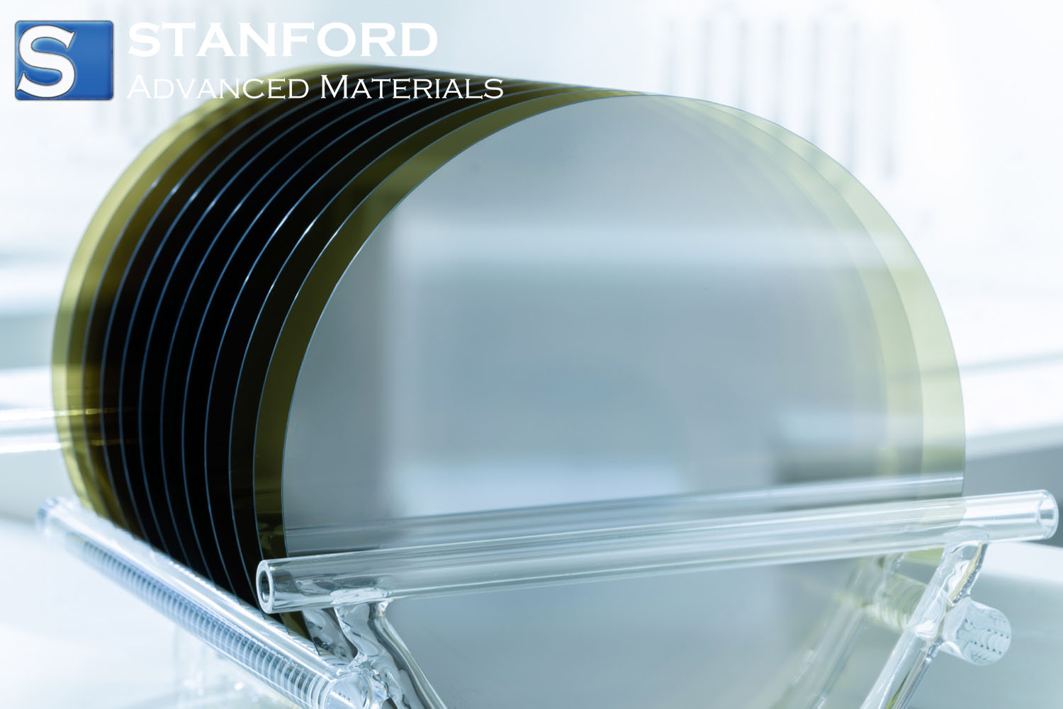
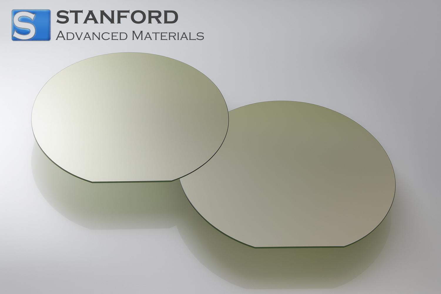
 Discs
Discs
 Fibers & Fabrics
 Films
Films
 Flake
Flake
 Foams
Foams
 Foil
Foil
 Granules
 Honeycombs
 Ink
Ink
 Laminate
 Lumps
Lumps
 Meshes
 Metallised Film
 Plate
Plate
 Powders
 Rod
Rod
 Single Crystals
 Sputtering Target
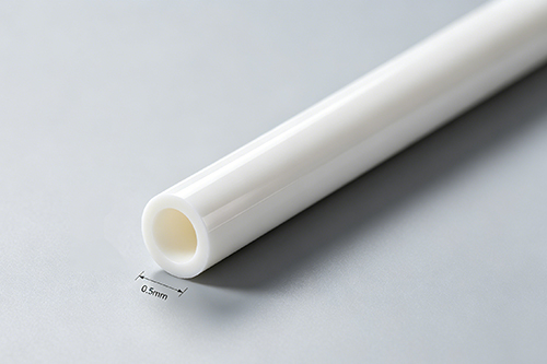
 Tubes
Tubes
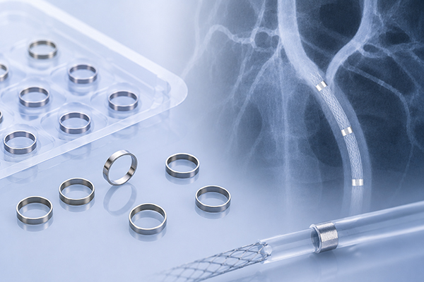
 Washer
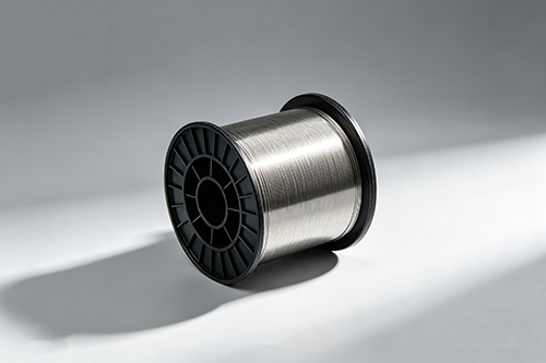
 Wires
Wires
 Converters & Calculators
 Write for Us

High Thermal Conductivity Silicon Carbide Wafer for Power Electronics in High-Voltage, High-Temperature Applications

Customer Background
A leading semiconductor manufacturer specializing in power electronics substrates was working to advance the performance of their high-voltage, high-temperature devices. With growing demand for power modules capable of operating under extreme conditions, the customer required silicon carbide (SiC) wafers that could serve as reliable substrates. Previous experiences with standard wafer supplies had revealed variability issues, especially in thermal performance and dimensional tolerances, which limited device reliability.
The customer engaged with our team, providing detailed RFQs and technical specifications. Their design demanded wafers with high thermal conductivity to dissipate heat efficiently and support devices operating above typical temperature thresholds. The engineering drawings detailed a requirement for a specific crystal orientation critical for heat transfer and a tight thickness tolerance to ensure compatibility with their power electronic packaging and bonding processes.
Challenge
The core challenge for the customer was to secure a silicon carbide wafer that met several stringent technical and operational requirements:
- Achieve a wafer purity of at least 99.9% to minimize defects that could negatively affect electron mobility.
- Maintain a thickness specification of approximately 350 µm with a tolerance of ±5 µm, ensuring uniform thermal distribution across the substrate.
- Optimize the crystal orientation (preferably along the <0001> axis) to maximize thermal conductivity, directly impacting the efficiency of the power electronics devices.
- Address the issue of bonding discontinuities; the selected wafers needed to be compatible with specific packaging methods and bonding agents, ensuring a stable interface during device operation.
- Navigate a strict lead time constraint. Previous suppliers had delayed delivery, leading to a bottleneck in the customer's manufacturing schedule and hampering overall production efficiency.
This combination of high material purity, precise dimensional control, and specialized crystal orientation presented a non-standard challenge that required advanced manufacturing capabilities and meticulous quality control.
Why They Chose SAM
The customer evaluated several suppliers, ultimately selecting Stanford Advanced Materials (SAM) after an extensive review of technical capabilities and process expertise. Our initial consultation went beyond a standard quotation. We provided in-depth feedback on potential thermal and bonding challenges that might arise from the specified crystal orientation and dimensional requirements.
Our team at SAM demonstrated:
- A track record of over 30 years supplying customized advanced materials with tailored specifications.
- A deep understanding of semiconductor material behaviors under high-voltage and high-temperature conditions.
- Flexibility in meeting tight production schedules without compromising quality, which was critical given the immediate lead time challenges faced by the customer.
This thoughtful and technically robust approach was instrumental in assuring the customer that we could deliver wafers meeting both their design requirements and operational constraints.
Solution Provided
SAM delivered a custom silicon carbide wafer solution designed explicitly for power electronics substrates. The following technical details were critical in re-engineering the customer's process:
1. We sourced silicon carbide material with a measured purity of 99.9%, ensuring minimal defect density to support high electron mobility. This level of purity was necessary to prevent undesired electrical behavior during device operation.
2. The wafers were produced with a target thickness of 350 µm, maintained within a tight tolerance of ±5 µm. Achieving this precision was essential to guarantee consistent thermal pathways and to ensure compatibility with the customer's bonding processes.
3. The crystal structure was oriented along the <0001> axis. This orientation was specifically selected for its superior thermal conductivity properties, which helped in managing the high thermal loads expected in high-voltage applications.
Additionally, bonding compatibility was a significant focus. SAM adjusted the surface finish and doping profiles to align with the customer's package bonding agents, thereby reducing the risk of delamination under thermal stress. Our advanced machining process ensured edge quality that met the customer's strict dimensional and microstructural standards.
To address the lead time constraints, we optimized our production workflow and supply chain logistics. This allowed us to deliver the wafers within the customer's narrow time window, circumventing issues that had affected previous supplier performance.
Results & Impact
The delivered silicon carbide wafers performed reliably during rigorous testing in power electronic substrate applications. The following outcomes were observed:
· Consistent film adhesion and bonding were achieved, thanks to the tightly controlled surface finish and optimal doping levels tailored for the customer's packaging process.
· The adherence to a crystal orientation along the <0001> axis resulted in improved heat dissipation. Measurably lower operating temperatures were recorded, contributing to heightened reliability in high-temperature, high-voltage operations.
· The strict thickness tolerance (350 µm ±5 µm) ensured uniform thermal distribution across the wafers, mitigating hotspots and reducing potential device failure rates.
· The customer's production line experienced fewer delays and lower scrap rates. This stability improved overall manufacturing efficiency and reduced the need for repeated material orders.
· Operational performance improved, with devices showing reduced variability in critical electrical parameters during extended high-temperature operation.
In summary, the solution not only addressed the technical challenges identified but also resolved supply chain constraints, positioning the customer for improved operational efficiency and consistency in device performance.
Key Takeaways
For manufacturers operating in the high-voltage, high-temperature domain, the detailed examination of technical parameters such as material purity, thickness tolerance, and crystal orientation is fundamental. Our approach at Stanford Advanced Materials (SAM) underscores the importance of:
- Precisely tailoring material properties to match demanding operational environments.
- Recognizing and acting on real-world constraints like lead times, which can significantly impact production.
- Providing customized solutions that address both bonding performance and thermal management challenges.
In our experience, engaging with suppliers who offer detailed technical feedback alongside flexible production capabilities can markedly improve end-device performance and operational efficiency. This case reinforces our commitment to providing tailored, reliable advanced materials with the precision required in demanding semiconductor applications.
 Dr. Samuel R. Matthews