Bars
Bars
 Beads & Spheres
 Bolts & Nuts
 Crucibles
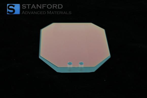
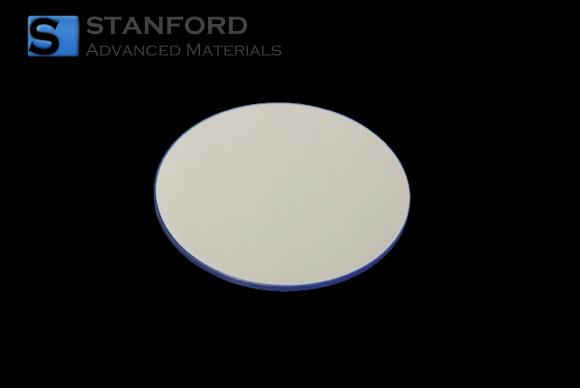
 Discs
Discs
 Fibers & Fabrics
 Films
Films
 Flake
Flake
 Foams
Foams
 Foil
Foil
 Granules
 Honeycombs
 Ink
Ink
 Laminate
 Lumps
Lumps
 Meshes
 Metallised Film
 Plate
Plate
 Powders
 Rod
Rod
 Single Crystals
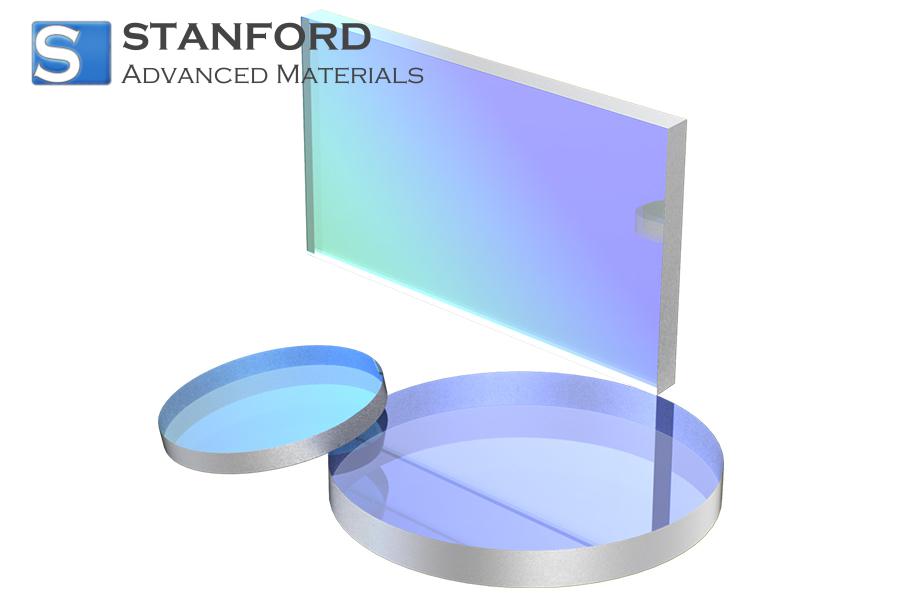
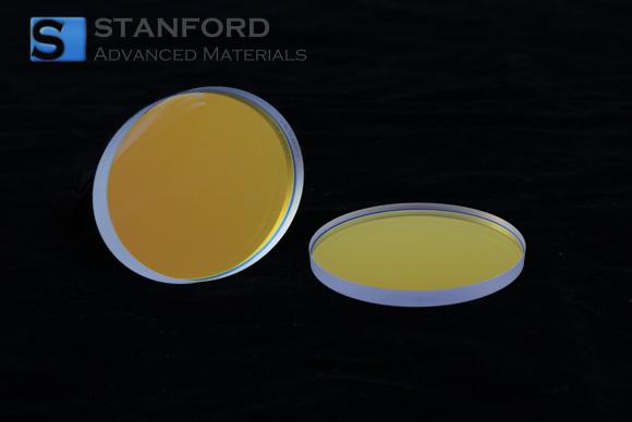
 Sputtering Target
 Tubes
Tubes
 Washer
 Wires
Wires
 Converters & Calculators
 Write for Us

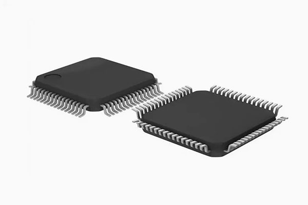
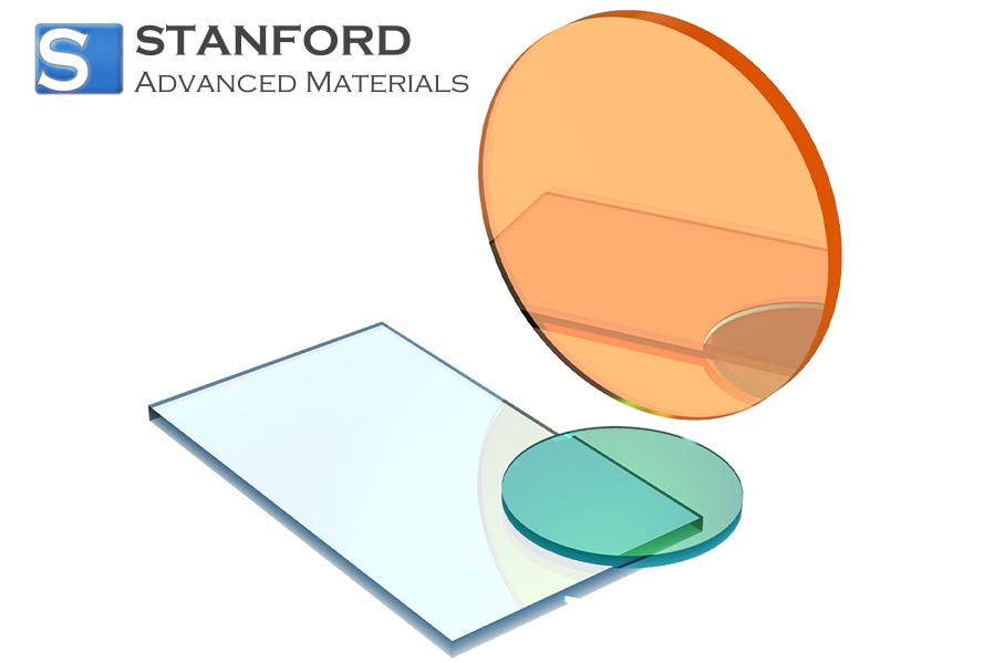
All about Semiconductor Chips and Metal Sputtering Targets

Description
Semiconductor chips form the backbone of modern electronics. They are found in everyday devices such as computers, mobile phones, and automobiles. These chips rely on thin films and coatings to improve performance and reliability. Metal sputtering targets are one of the key tools in producing these films. They are highly pure metal pieces processed to strict standards.
Why
The purpose of using metal sputtering targets in semiconductor chip production is twofold. First, they offer an efficient way to deposit thin films with controlled thickness. Second, they allow for deposition of films with excellent adhesion and conductivity. For example, a chip needing a copper interconnect relies on a copper target that provides excellent electrical pathways.
Using these targets provides consistency. They assure that each film deposition is uniform. This is important in high-volume manufacturing. The stability of the process helps technicians maintain high yields. In addition, the physical properties of the sputtered film, such as low resistivity and good barrier properties, are essential for chip performance. In many applications, even a slight deviation from the norm could lead to potential failures.
Where
Metal sputtering targets are predominantly used in semiconductor fabrication plants. These facilities have advanced cleanrooms where air purity and temperature are closely controlled. In these plants, targets see application in deposition chambers that are dedicated to the thin film deposition process.
Beyond chip fabrication, sputtering targets can be found in research laboratories. In these settings, the targets support the development of new film materials. Academic and industrial labs use sputtering to test novel compounds and film structures. Semiconductor production facilities often schedule regular replacements of targets. This ensures that no contaminants affect the quality of the deposited films.
The sputtering process also finds its place in display manufacturing and solar cell production. In each of these sectors, the targets provide materials that support the unique requirements of the final product. Clean environments and precise control measures ensure the correct properties are achieved every time.
Other Sputtering Targets Used for Semiconductor Chips
Metal sputtering targets are not limited to copper or aluminum. Several other materials have found their way into semiconductor device production. For instance, tungsten targets are used where high temperature resilience is needed. Tungsten films provide excellent stability and low resistivity. Titanium and its alloys serve in situations that require strong adhesion between layers. Several processes use titanium to improve the bond between different materials.
Oxide targets are frequently employed in semiconductor fabrication as well. Metals such as indium tin oxide are sputtered to produce transparent conductive films. These materials appear in displays and touch screens. Nitride and carbide targets also have applications in semiconductor devices, especially when hardness and wear resistance are important. Each of these materials brings its own set of benefits to the thin film deposition process. They allow for fine adjustments to meet the design specifications of modern electronic components.
Research and development in the field continue to push the limits of material usage. As new compounds are introduced, the library of sputtering targets expands. This continuous flow of innovation helps meet specific performance needs across the industry. Companies collaborate with suppliers to ensure that target properties are tailored precisely to the manufacturing process.
Conclusion
Semiconductor chips form the heart of modern technology. Metal sputtering targets play an essential role in their production. These targets provide high purity, uniform films critical for electrical performance and longevity. For more sputtering targets, please check Stanford Advanced Materials (SAM).
Frequently Asked Questions
F: What role do sputtering targets play in semiconductor manufacturing?
Q: They deposit uniform, high-purity films essential for forming reliable semiconductor circuits.
F: Which metals are commonly used in sputtering targets for chips?
Q: Copper, aluminum, titanium, and tungsten are among the most common metals used.
F: How do sputtering targets affect chip performance?
Q: They ensure consistent thin films which lead to improved electrical conductivity and device reliability.
 Chin Trento