Bars
Bars
 Beads & Spheres
 Bolts & Nuts
 Crucibles
 Discs
Discs
 Fibers & Fabrics
 Films
Films
 Flake
Flake
 Foams
Foams
 Foil
Foil
 Granules
 Honeycombs
 Ink
Ink
 Laminate
 Lumps
Lumps
 Meshes
 Metallised Film
 Plate
Plate
 Powders
 Rod
Rod
 Single Crystals
 Sputtering Target
 Tubes
Tubes
 Washer
 Wires
Wires
 Converters & Calculators
 Write for Us

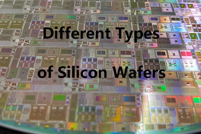
Different Types of Silicon Wafers

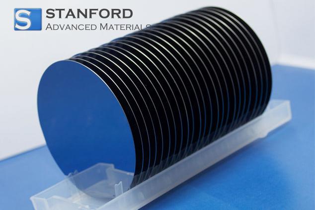
Many people have probably worked with silicon wafers without even noticing it. Anybody who has ever had a computer or a mobile phone has probably relied on silicon wafers before. As one of the main suppliers of silicon wafers on the market, Stanford Advanced Materials (SAM) gets asked questions like "What is a silicon wafer? Or "What kind of silicon wafer shall I purchase for this purpose?" All of these will be answered by this complete guide to silicon wafers.
SAM provides a multitude of customized silicon wafers such as prime wafers, test wafers, and reclaimed wafers. Based on different parameters such as Orientation Crystals, Resistivity, Thickness, and Diameter, they make sure that consumers get hold of a suitable wafer for their needs.
Silicon Wafers by Crystal Structure
The silicon wafer crystal structure has been found to affect its electrical, mechanical, and thermal properties.
- Monocrystalline Silicon Wafers: These wafers are made from a single crystal and ensure consistent electrical properties with fewer defects. While Czochralski wafers cater to IC applications as well as high-efficiency solar cells, FZ wafers with extremely low impurities find their applications in high-power electronics, RF components, and high-voltage devices.
- Polycrystalline Silicon Wafers: These are produced from multiple crystal formations to save on cost, though they are not as uniform as single crystal wafers. These wafers are used in solar panels and other economical semiconductor devices.
- Amorphous Silicon Wafers: Used for making thin films such as TFT display screens, image sensors, and thin film solar cells.
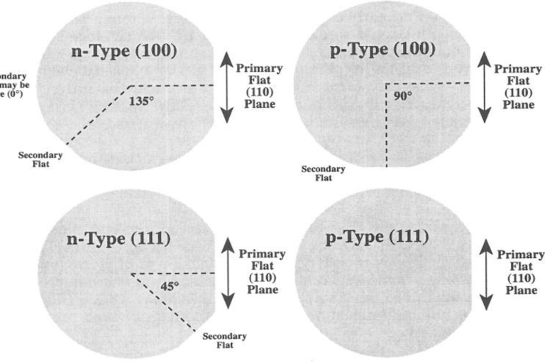
Silicon Wafers by Orientation
Crystalline orientation is important for wafer processing and etching. SAM supplies wafers with the most popular orientations:
- ⟨100⟩ Wafers - Suitable for oxidation and etching, excellent for CMOS logic, DRAM, and general IC processing.
- ⟨110⟩ Wafers – Selected for MEMS and anisotropic etch applications.
- ⟨111⟩ Wafers - Preferred for MEMS, sensors, and power devices where improved mechanical strength is required.
[1]
Silicon Wafers Based on Doping Types
"Doping" modifies the electrical properties of a semiconductor wafer through
- P-Type Wafers - Boron-doped wafers mostly used in solar cells and CMOS technology.
- N-Type Wafers - Phosphorus or arsenic doped, uses electrons as charge carriers, thus more mobile and resistant to ionizing radiation.
- Resistivity Variations - SAM can supply wafers from lightly doped to heavily doped according to device specifications, such as high resistivity wafers that can be used for RF technology or low resistivity wafers that can be employed in power electronics.
Surfaced Finish & Special Engineering
The wafer's surface characteristics and engineering make it ideal for sophisticated applications.
- Highly polished wafers - Single-side or double-side polished wafers for ICs, MEMS, or photonics.
- Lapped or Etched Wafers - Moderate surface finish, often used for R&D applications and power devices.
- SOI (Silicon on Insulator) Wafers - Parasitic capacitance reduced for RF, LP, and automotive applications.
- Ultra Thin Wafers - Thickness less than 100µm; mostly for Flexible Electronics and the packaging of 3D integration.
Related reading: Comparing SOI vs. Silicon Wafers: What's Best for Your Semiconductor Project?
Summary Table: Different Kinds of Silicon Wafers
|
Silicon Wafer Type |
Crystal Structure / Orientation |
Doping / Resistivity |
Surface Finish |
Typical Applications |
|
Monocrystalline (CZ) |
Single crystal, ⟨100⟩ or ⟨111⟩ |
P-type or N-type, standard resistivity |
Polished (SSP/DSP) |
ICs, CMOS logic, high-efficiency solar cells |
|
Monocrystalline (FZ) |
Single crystal, ⟨100⟩ |
Ultra-low impurities, high resistivity |
Polished |
High-power electronics, RF devices, high-voltage ICs |
|
Polycrystalline |
Multi-grain |
P-type or N-type, moderate resistivity |
Lapped or polished |
Photovoltaics, cost-sensitive semiconductors |
|
Amorphous Silicon (a-Si) |
Non-crystalline |
Lightly doped |
Thin-film surface |
TFT displays, thin-film solar cells, image sensors |
|
SOI (Silicon-on-Insulator) |
Monocrystalline layer on insulating layer |
P-type or N-type, variable resistivity |
Polished |
RF ICs, low-power devices, automotive electronics |
|
Ultra-Thin Wafers |
Single or polycrystalline |
P-type or N-type, custom resistivity |
Polished |
Flexible electronics, advanced packaging, 3D integration |
This table is an at-a-glance summary of various important characteristics of different silicon wafers so that you know which product is needed by you. SAM's experience as a reputed silicon wafer supplier ensures that all silicon wafers are of highest quality.
Conclusion
Silicon wafers represent a cornerstone for modern electronics, whether it is a common device, a computer, a micro-electromechanical system, or solar cells. The variety of orientations, doping types, surface finishes, and engineering features plays a key role in informed decision-making.
By procuring high-quality silicon wafers from a reputable silicon wafer supplier such as SAM, manufacturers and researchers are able to get silicon wafers that meet specific requirements, thereby allowing for optimal innovation within the semiconductor industry.
Reference:
[1] Mohd Said, Nur Azura & Ogurtsov, Vladimir & Herzog, Grégoire. (2014). ELECTROCHEMICAL BIOSENSOR BASED ON MICROFABRICATED ELECTRODE ARRAYS FOR LIFE SCIENCES APPLICATIONS. 10.13140/RG.2.2.11066.49603.
 Dr. Samuel R. Matthews