Bars
Bars
 Beads & Spheres
 Bolts & Nuts
 Crucibles
 Discs
Discs
 Fibers & Fabrics
 Films
Films
 Flake
Flake
 Foams
Foams
 Foil
Foil
 Granules
 Honeycombs
 Ink
Ink
 Laminate
 Lumps
Lumps
 Meshes
 Metallised Film
 Plate
Plate
 Powders
 Rod
Rod
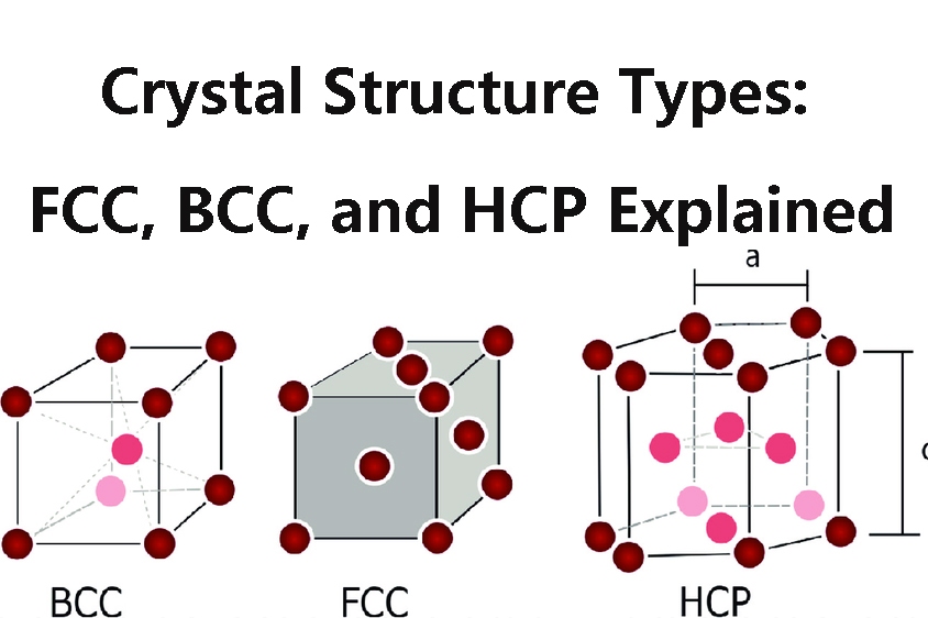
 Single Crystals
 Sputtering Target
 Tubes
Tubes
 Washer
 Wires
Wires
 Converters & Calculators
 Write for Us

Nernst Coefficient and Thermoelectric Effect

Introduction to the Nernst Effect
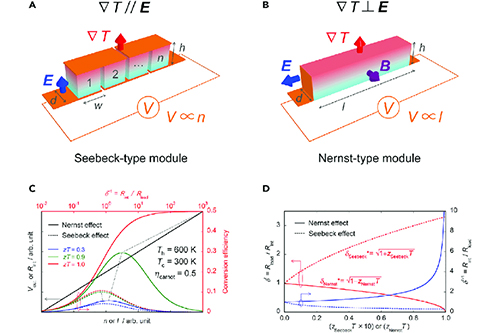
The Nernst Effect is a phenomenon observed in conductive materials when they are subjected to both a temperature gradient and a perpendicular magnetic field. This effect results in the generation of a transverse voltage, which is perpendicular to both the temperature gradient and the magnetic field. The Nernst coefficient is a parameter that quantifies the magnitude of this transverse voltage relative to the applied fields.
Physical Origin
The Nernst effect arises from the motion of charge carriers under crossed thermal and magnetic fields. When a temperature gradient is applied along a sample, charge carriers diffuse from the hot end to the cold end. In the presence of a perpendicular magnetic field, these moving carriers experience a Lorentz force, deflecting them to the sample edges. This charge buildup creates a transverse electric field—the Nernst voltage. The magnitude of this voltage depends on how easily carriers are deflected, which is related to their mobility and scattering rates.
Mathematically, the Nernst coefficient (N) is defined through the relation:
E_y = N · B_z · ∇_x T
where E_y is the transverse electric field, B_z is the applied magnetic field, and ∇_x T is the temperature gradient along the sample.
Introduction to the Thermoelectric Effect
The thermoelectric effect encompasses various phenomena where temperature differences within a material generate electric voltages or vice versa. It includes the Seebeck effect, Peltier effect, and the Nernst effect. These effects are harnessed in applications such as power generation, refrigeration, and temperature sensing.
While the Seebeck and Peltier effects are widely used in commercial devices, the Nernst effect remains primarily a research tool—though interest is growing due to its sensitivity to material properties and its potential in magnetic field sensing and energy harvesting.
Applications of the Nernst Coefficient
The Nernst coefficient plays a pivotal role in several advanced applications:
Material Characterization
By measuring the Nernst coefficient, researchers can gain insights into the electronic properties of materials, including carrier concentration and mobility.
Magnetic Field Sensing
The sensitivity of the Nernst effect to magnetic fields makes it useful in designing precise magnetic field sensors.
Thermoelectric Devices
In thermoelectric generators and coolers, understanding the Nernst coefficient helps in optimizing device performance under varying magnetic and thermal conditions.
Factors Influencing the Nernst Coefficient
Several factors affect the Nernst coefficient in materials:
- Temperature: Higher temperatures can enhance phonon interactions, influencing the Nernst response.
- Magnetic Field Strength: The magnitude of the applied magnetic field directly affects the generated transverse voltage.
- Material Composition: Different materials exhibit varying Nernst coefficients based on their electronic structure and carrier dynamics.
- Crystal Structure: The symmetry and lattice structure of a material can enhance or suppress the Nernst effect.
Comparison with Other Thermoelectric Effects
| Thermoelectric Effect | Description | Key Coefficient | Field Required |
|---|---|---|---|
| Seebeck Effect | Generation of longitudinal voltage from a temperature gradient | Seebeck coefficient (S) | No |
| Peltier Effect | Absorption or release of heat when current flows | Peltier coefficient (Π) | No |
| Nernst Effect | Transverse voltage from temperature gradient and magnetic field | Nernst coefficient (N) | Yes |
The Nernst effect differs fundamentally from the Seebeck effect in both its origin and its information content. While the Seebeck effect is sensitive to the density of states and carrier concentration, the Nernst effect responds primarily to carrier mobility. This makes the two measurements complementary—together, they provide a more complete picture of electronic transport.
Materials for Nernst Effect Research from SAM
Stanford Advanced Materials (SAM) supplies high-purity materials used in thermoelectric and Nernst effect research, including:
- Semiconductors: InSb, InAs, HgCdTe, and others
- Metals and semimetals: Bismuth, antimony, tellurium, and high-purity metals
- Oxides and chalcogenides: For thermoelectric and topological material studies
- Single crystals: Various materials available in crystalline form for anisotropic studies
Available forms include polycrystalline ingots, single crystals, powders, and custom substrates.
[Browse our materials] or [contact us] for specific requirements.
Frequently Asked Questions
What distinguishes the Nernst effect from the Seebeck effect?
The Nernst effect generates a transverse voltage in the presence of both a temperature gradient and a magnetic field, whereas the Seebeck effect produces a voltage solely from a temperature gradient.
How is the Nernst coefficient measured?
It is measured by applying a known temperature gradient and magnetic field to a material and then measuring the resulting transverse voltage.
In which materials is the Nernst effect most prominent?
The Nernst effect is particularly significant in materials with high mobility charge carriers, such as certain semiconductors and superconductors.
Can the Nernst effect be utilized in energy harvesting?
Yes, it can contribute to thermoelectric energy harvesting, especially in environments where magnetic fields are present.
How does the magnetic field influence the Nernst coefficient?
A stronger magnetic field typically enhances the Nernst coefficient by increasing the transverse voltage generated for a given temperature gradient.

 Chin Trento